Micro-BGA beam lead connection with cantilevered beam leads

a technology of cantilevered beam leads and micro-bga beams, which is applied in the direction of semiconductor devices, semiconductor/solid-state device details, electrical apparatus, etc., can solve the problems of .mu.bga packaging not being as robust, reducing the flexibility of the package, and reducing the design, manufacture and reliability of the die packaging. achieve the effect of avoiding the potential for short circuit and increasing flexibility

Inactive Publication Date: 2003-02-04
ADVANCED MICRO DEVICES INC
View PDF9 Cites 3 Cited by
  • Summary
  • Abstract
  • Description
  • Claims
  • Application Information

AI Technical Summary

Benefits of technology

Accordingly, a need exists in the art for an improved ball grid array package that avoids a potential for short circuit due to beam lead support placement and provides additional flexibility in bonding pad and beam lead placement.

Problems solved by technology

These semiconductor devices are typically small and fragile and commonly carried on substrates or carrier members for support.
However, despite its advantages, .mu.BGA packaging is not as robust as conventional packaging and die evolution to increasingly smaller die sizes, particularly to CSPs, imposes additional constraints on design, manufacture and reliability of the die packaging.
If the bending profile, such as the radius of curvature of the points of beam inflection, is too severe hairline cracks may develop and lead to device failure.

Method used


Image

  • Micro-BGA beam lead connection with cantilevered beam leads
  • Micro-BGA beam lead connection with cantilevered beam leads
  • Micro-BGA beam lead connection with cantilevered beam leads

Examples


Embodiment Construction

The present invention addresses and solves problems related to .mu.BGA short circuit caused by improper beam lead support placement and provides additional flexibility in bonding pad and beam lead placement.

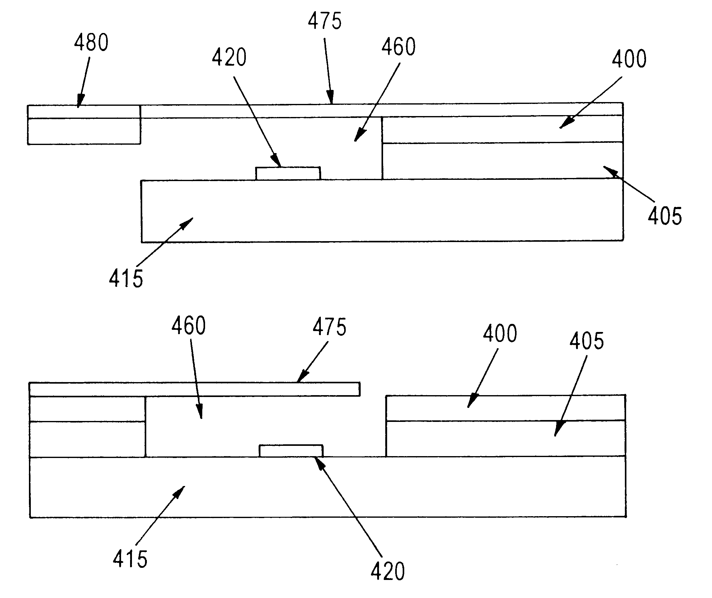
FIG. 4 depicts a top view of a tape automated bonding (TAB) tape according to the invention and FIGS. 5a and 5b show illustrative cross-sections thereof. The TAB tape 400 includes a die receiving section 410 for receiving a die 415, such as a FLASH memory die or other form of semiconductor chip, possessing a plurality of bonding pads 420 on a side of die opposing the tape 400. The tape 400 is connected to this die 415 by conventional connecting agents, such as adhesives, which are preferably used in combination with a compliant elastomer 405, such as an epoxy thermoset, disposed between the tape 400 and die 415, as shown in FIG. 5b. The elastomer provides a buffer against thermal and mechanical stresses and strains caused by varying coefficients of thermal expansion between the t...


PUM


Abstract

A tape automated bonding (TAB) tape is provided with an insulating tape having a die receiving section. The TAB tape also has a conductive wiring pattern forming a plurality of traces including a land at one end and a beam lead at another end. A tape window is formed in a portion of the tape die receiving section. At least one trace beam lead extends over the tape window from a first direction and is connected to a tie bar adjacent an opposing side of the tape window and at least one trace beam lead extends over the tape window from a second direction different than the first direction and is cantilevered over the tape window.

Description

The present invention relates to integrated circuit packages, and more particularly to an integrated circuit package having beam leads approaching die bonding pads from more than one direction.Semiconductor chips or wafers are used in applications including integrated circuits (ICs) or flash memory, which may be used in portable electronic devices. It is desirable that a semiconductor chip hold as many circuits or memory cells as possible per unit area to minimize the size, weight, and energy consumption of devices using the semiconductor chips. ICs, whether individual active devices, individual passive devices, multiple active devices within a single chip, or multiple active and passive devices within a single chip, require suitable input / output (I / O) connections between themselves and other circuit elements or structures. These semiconductor devices are typically small and fragile and commonly carried on substrates or carrier members for support. These devices are also frequently ...

Claims


Application Information

Patent Timeline
IPC IPC(8): H01L23/48H01L23/498
CPCH01L23/4985H01L2924/0002H01L2924/00
Inventor FONTECHA, EDWIN R.VALLURI, VISWANATHVIVARES, VALERIE
Owner ADVANCED MICRO DEVICES INC
Why Eureka
Try Eureka