Semiconductor memory device, and read method and read circuit for the same

a memory device and memory technology, applied in the field of memory devices of semiconductors, can solve the problems of affecting the read determination operation, blocking stable read operation, controlling parallel operation, etc., and achieve the effect of shortening the read cycle and simple circuit configuration

Inactive Publication Date: 2008-01-10
PANASONIC SEMICON SOLUTIONS CO LTD
View PDF8 Cites 20 Cited by
  • Summary
  • Abstract
  • Description
  • Claims
  • Application Information

AI Technical Summary

Benefits of technology

[0051]In the semiconductor memory device according to the present invention, a plurality of stages of serially connected column selection circuits and parallel connecte

Problems solved by technology

If the address changes in this state to select a word line connected with memory cells MC all having data “1”, the residual charge in the bit lines will be discharged at one time via the memory cells MC, causing a malfunction due to noise.
However, a problem arises in the control of the parallel operation of the bit line residual discharge in a given read cycle with the

Method used


Image

  • Semiconductor memory device, and read method and read circuit for the same
  • Semiconductor memory device, and read method and read circuit for the same
  • Semiconductor memory device, and read method and read circuit for the same

Examples


embodiment 1

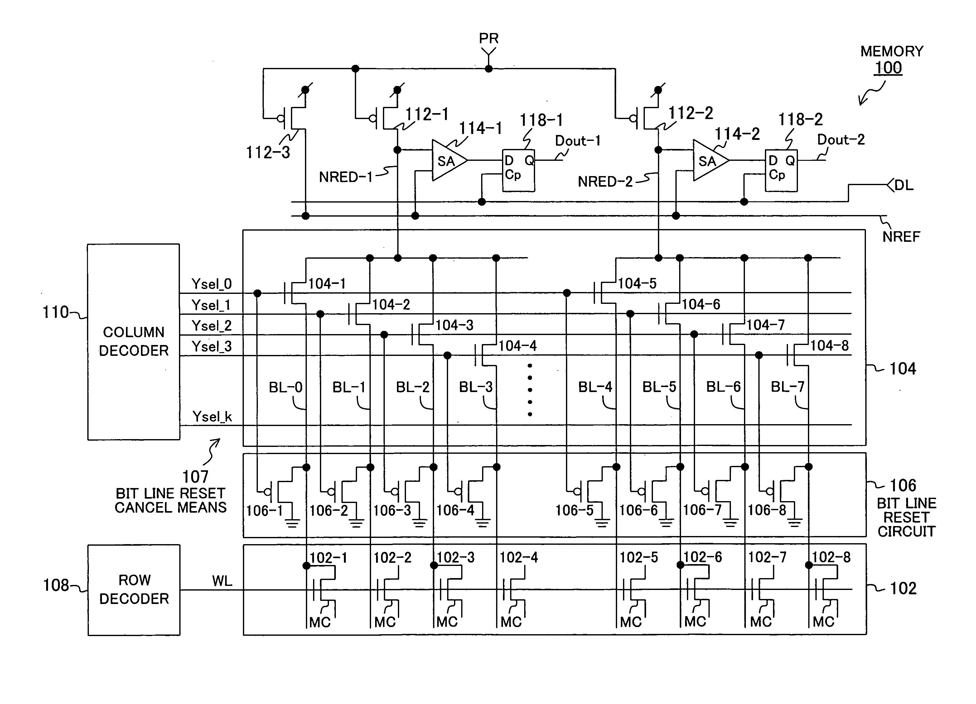
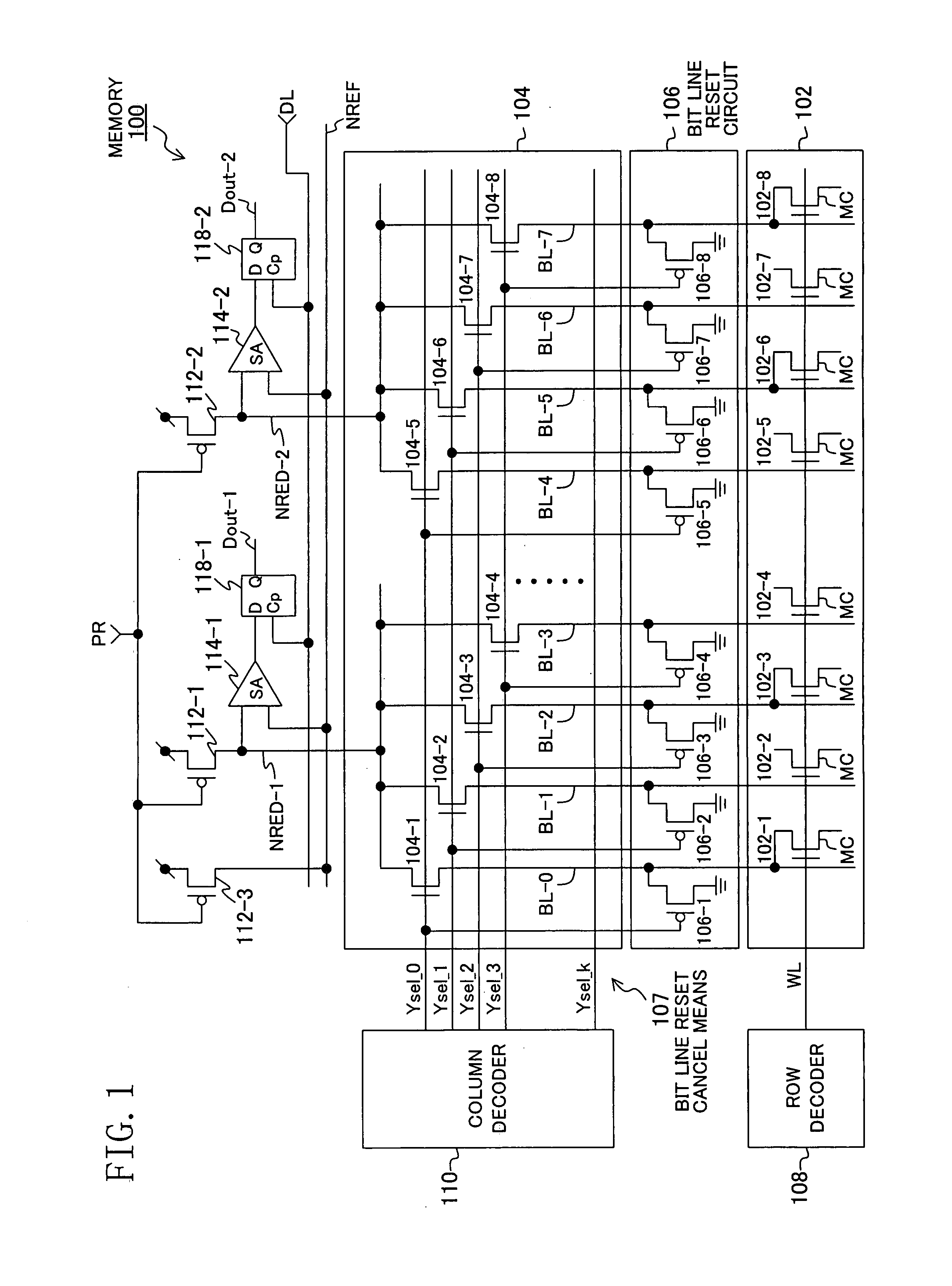
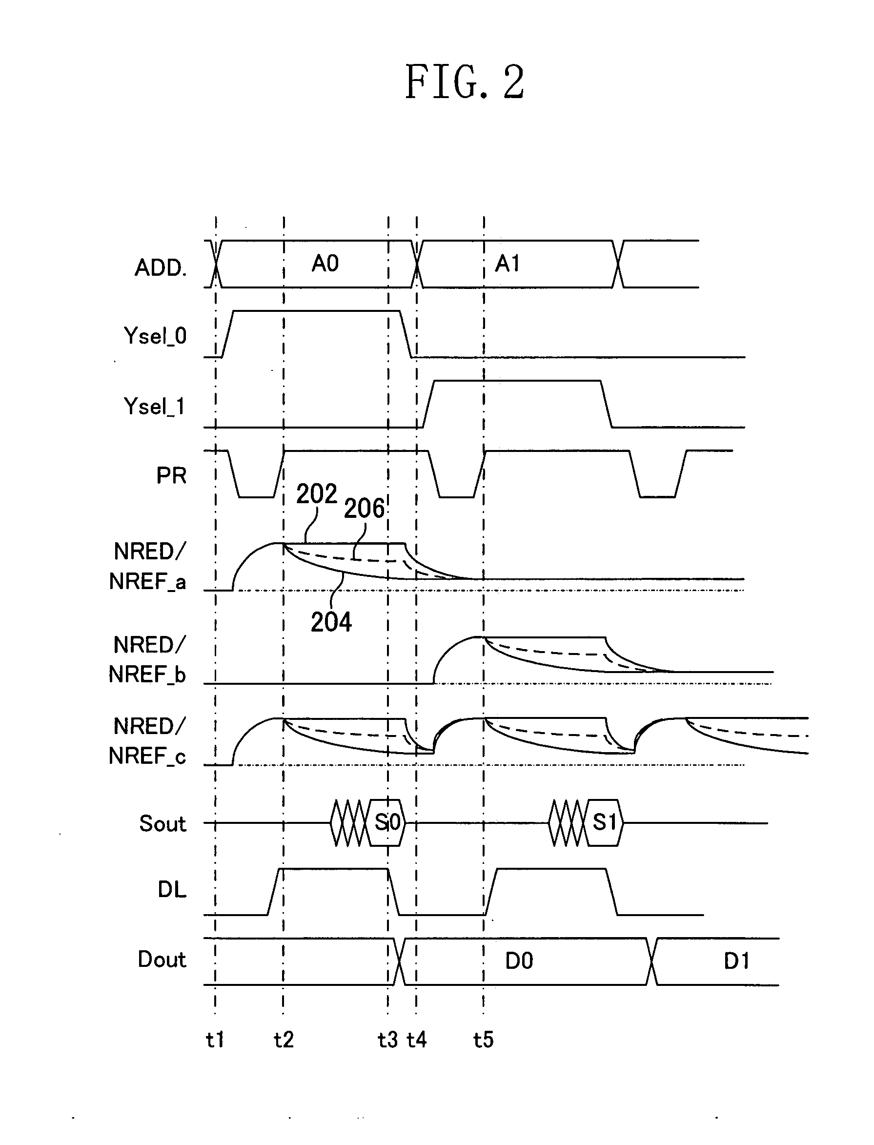
[0064]FIG. 1 shows an exemplary configuration of a semiconductor memory device of Embodiment 1 of the present invention, in which identical circuit components to those in FIG. 7 are denoted by the same reference numerals. A memory 100 includes a row decoder 108 and a column decoder (selection signal generation circuit) 110. The row decoder 108 selects one of word lines WL running in a memory cell array 102 in response to a row address received externally, to apply a read voltage to the gate electrodes of memory cells MC 102-1 to 102-8. The column decoder 110 generates and outputs bit line selection signals Ysel_0 to Ysel_k for driving a column selection gate 104 in response to a column address received externally. N-channel selection transistors 104-1 to 104-8 in the column selection gate (connection circuit and column selection circuit) 104, driven with the bit line selection signals Ysel_0 to Ysel_k from the column decoder 110, selectively connect bit lines BL-0 to BL-7 that are c...

embodiment 2

[0073]In the configuration shown in FIG. 1, the selection transistors 104-1 to 104-8 in the column selection gate 104 are N-channel transistors while the bit line reset circuit 106 is composed of the P-channel transistors 106-1 to 106-8, so that the selection signals Ysel_0 to Ysel_k from the column decoder 110 can be used, as common control signals. In this configuration, however, since the bit line reset circuit 106 composed of the P-channel transistors performs the discharge to the ground potential, the potential equal to the threshold voltage of the P-channel transistors remains as the bit line potential after the reset. Therefore, the effect of noise discussed in the prior art problem, which occurs when charge remains in a number of bit lines and the residual charge is discharged at one time via memory cells at the time of transition to a different word line, remains to some extent.

[0074]FIG. 3 shows an exemplary circuit configuration in which the residual charge after the bit ...

embodiment 3

[0078]In FIGS. 1 and 3, shown were examples where the column selection gates 104 and 302 were composed of one stage of the selection transistors 104-1 to 104-8 and 302-1 to 302-8 connected to the bit lines. The column selection gate may otherwise be composed of a plurality of serially connected stages for the purpose of reducing the number of bit line selection signals from the column decoder 110 required.

[0079]FIG. 5 shows an exemplary memory configuration in which the column selection gate is composed of two serially connected stages of selection transistors. In a memory 500 shown in FIG. 5, the column selection gate has a two-stage structure including a first column selection gate (first column selection circuit) 505 composed of first N-channel transistors 505-1, 505-2, 505-5 and 505-6 and a second column selection gate (second column selection circuit) 506 composed of second N-channel transistors 506-1 and 506-2. The N-channel transistors are respectively driven with bit line se...


PUM


Abstract

In a semiconductor memory device operative to discharge residual charge in a read bit line in a read cycle, the bit line is in the reset state at all times except during read operation. The reset state of a bit line is canceled when selected and connected to a read circuit for read, and information stored in a selected memory cell is read via the selected bit line. Upon completion of the read of the memory cell, the selected bit line is disconnected from the read circuit and reset to thereby complete discharge of residual charge in the read bit line prior to read operation in the next cycle. This ensures that during read determination operation in the next read cycle, the potential of a selected bit line will not vary with the bit line residual discharge in the previous read cycle.

Description

CROSS-REFERENCE TO RELATED APPLICATIONS[0001]This non-provisional application claims priority under 35 U.S.C. §119(a) on Patent Application No. 2006-185870 filed in Japan on Jul. 5, 2006, the entire contents of which are hereby incorporated by reference.BACKGROUND OF THE INVENTION[0002]The present invention relates to a semiconductor memory device, and more particularly, to a technology effectively applicable to readout of a semiconductor memory device in which a number of memory cells are connected to one bit line and the bit line capacitance is large.[0003]In general, nonvolatile memories such as mask ROMs, PROMs and EPROMs store information by setting each memory cell at either of two states allowing and not allowing current flow between its source and drain when a read voltage is applied.[0004]FIG. 7 shows an exemplary configuration of a mask ROM. A memory 700 includes a memory cell array 102 having memory cells arranged in a matrix. FIG. 8 shows a specific circuit configuration...

Claims


Application Information

Patent Timeline
IPC IPC(8): G11C8/08G11C11/34G11C8/10
CPCG11C16/28G11C16/24
Inventor MORI, TOSHIKI
Owner PANASONIC SEMICON SOLUTIONS CO LTD
Why Eureka
Try Eureka