Operable synchronous semiconductor memory device switching between single data rate mode and double data rate mode

a semiconductor memory and data rate technology, applied in the field of semiconductor integrated circuit devices, can solve the problems of increasing the cost required for designing and manufacturing

Inactive Publication Date: 2003-02-18
DRAM MEMORY TECH
View PDF13 Cites 49 Cited by
  • Summary
  • Abstract
  • Description
  • Claims
  • Application Information

AI Technical Summary

Problems solved by technology

When a SDRAM designed to correspond to a system that requires maximum speed is used in a system that allows a lower operating frequency, it is not desirable from the standpoint of power consumption to operate the SDRAM according to the specification of the highest speed.
If a different design is to be provided according to each particular application, the cost required for designing and fabrication will increase.

Method used


Image

  • Operable synchronous semiconductor memory device switching between single data rate mode and double data rate mode
  • Operable synchronous semiconductor memory device switching between single data rate mode and double data rate mode
  • Operable synchronous semiconductor memory device switching between single data rate mode and double data rate mode

Examples


first embodiment

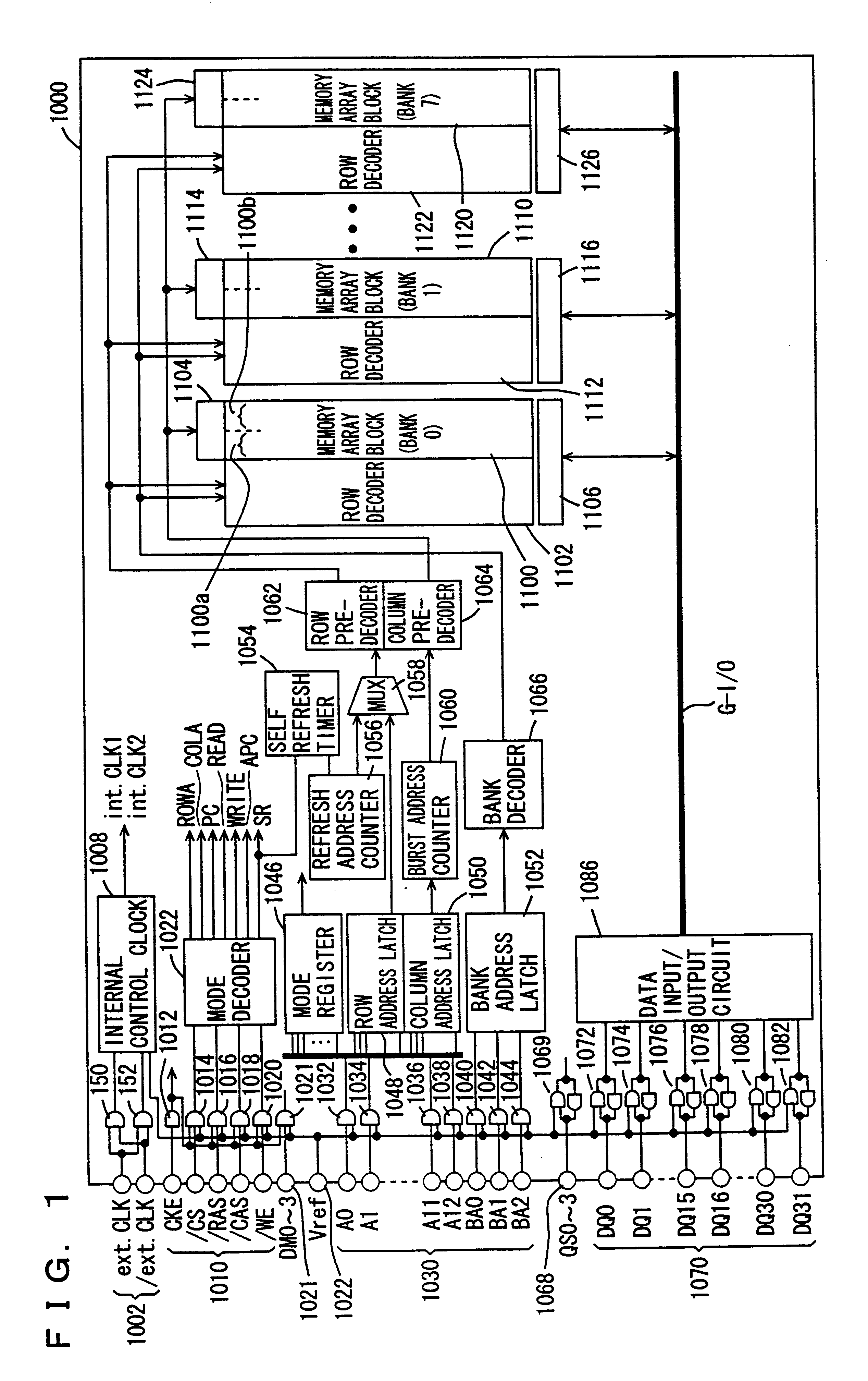
FIG. 1 is a schematic block diagram showing a structure of a synchronous semiconductor memory device 1000 according to the present invention.

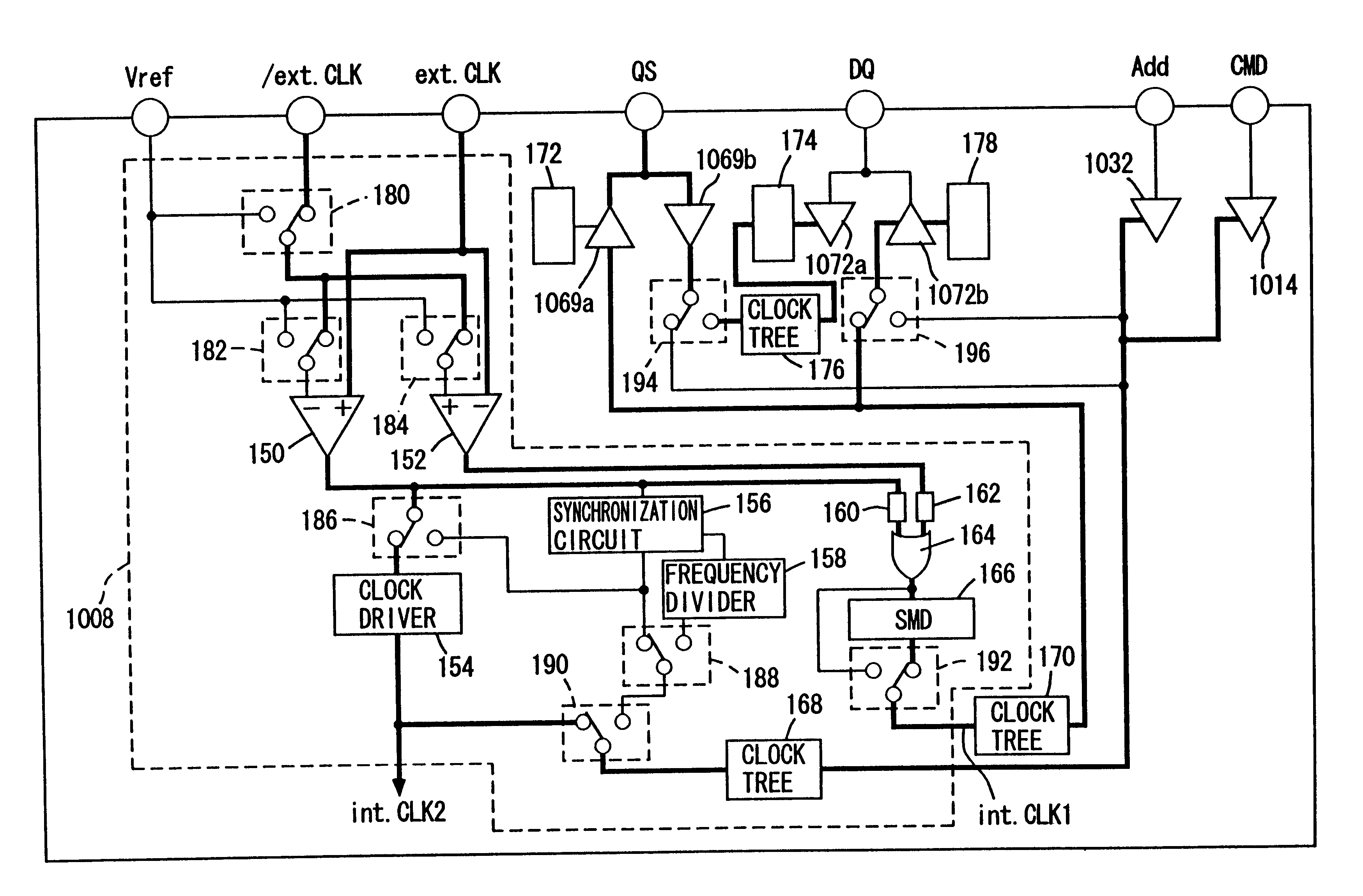
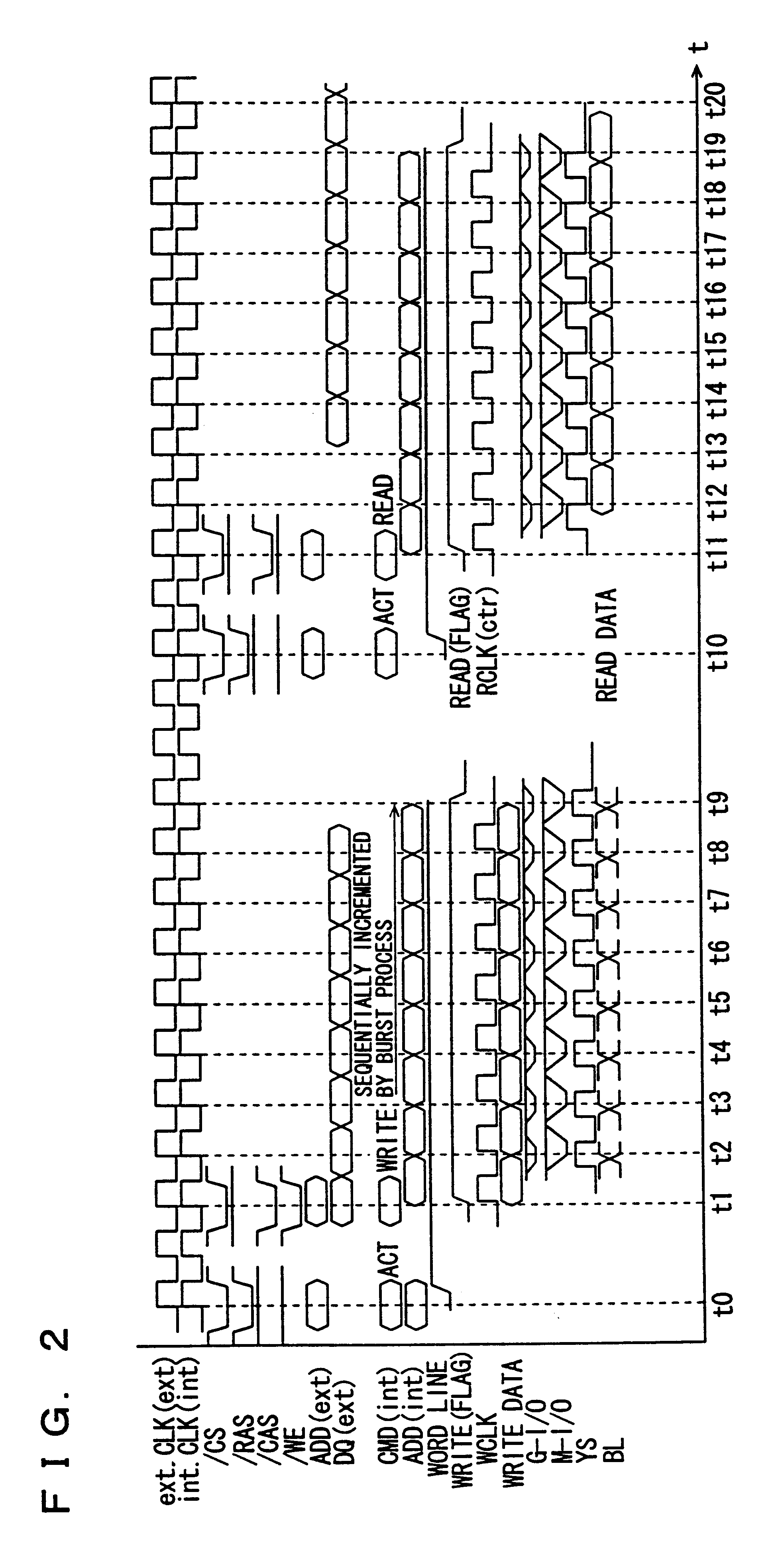
SDRAM 1000 includes an external clock signal input terminal 1002 receiving externally applied complementary clock signals ext.CLK and ext. / CLK, clock input buffers 150 and 152 applying a buffer process on a clock signal applied to external clock terminal 1002, an internal control clock signal generation circuit 1008 receiving the outputs of clock buffers 150 and 152 to generate a first internal clock signal int.CLK1 and a second internal clock signal int.CLK2, and a mode decoder 1002 receiving via input buffers 1012-1020 that operate according to second internal signal int.CLK2 an external control signal provided via an external control signal input terminal 1010.

A signal CKE, a chip select signal / CS, a row address strobe signal / RAS, a column address strobe signal / CAS, a write control signal / WE, and data mask signals DM0-DM3 are applied to ...

second embodiment

FIG. 18 is a schematic block diagram showing a structure of a synchronous semiconductor memory device 2000 according to a second embodiment of the present invention.

Referring to FIG. 18, synchronous semiconductor memory device 2000 includes a control circuit 20 receiving and decoding external control signals / RAS, / CAS, / W, / CS and the like applied via external control signal input terminal group 10 to generate an internal control signal, command data buses 53a and 53b for transmitting the internal control signal output from control circuit 20, and a memory cell array 1000 in which memory cells are arranged in a matrix.

Memory cell array 100 is divided into a total of 16 memory cell blocks 100a-100p as shown in FIG. 18. When synchronous semiconductor memory device 2000 has a storage capacity of 1 Gbits, for example, each memory cell block has a capacity of 64 Mbits. Each block can operate as an independent bank.

Synchronous semiconductor memory device 2000 further includes an internal...

third embodiment

Modification of Third Embodiment

FIG. 33 shows a structure of a SDRAM in the case where the data input / output terminal group and the output control circuit are arranged in the proximity of bank 100d, i.e., near the center of the chip.

Data is transmitted from the center circuit portion of the SDRAM to respective banks through the clock bus, command bus, address bus, and data bus.

The address data and command data are transmitted most earliest at bank 100d that is located closest to the center circuit portion. Therefore, when bank 100d initiates its operation to output data, for example, in a readout operation, the data readout from bank 100d will be output towards the data input / output terminal at an early time point.

In contrast, the transmission of an address signal and a command signal is latest for bank 100a that is located most remote from the center circuit portion. The readout data is output later than the output from bank 100d. Bank 100a is located further away with respect to t...


PUM


Abstract

A synchronous semiconductor memory device operates an input/output buffer circuit in synchronization with an external clock signal in a single data rate SDRAM operation mode. In a double data rate SDRAM operation mode, an internal clock signal of a frequency two times that of the external clock signal is generated. The input/output buffer circuit is operated in synchronization with the internal clock signal.

Description

1. Field of the InventionThe present invention relates to semiconductor integrated circuit devices, and particularly to a semiconductor integrated circuit device that operates in synchronization with an external clock signal. More particularly, the present invention relates to, for example, a synchronous semiconductor memory device that operates in synchronization with an external clock signal.2. Description of the Background ArtIn accordance with increase in the operating speed of recent microprocessors (referred to as MPU hereinafter), a synchronous DRAM that operates in synchronization with a clock signal and the like (synchronous DRAM: referred to as SDRAM hereinafter) are used to realize high speed access of dynamic random access memories (referred to as DRAM hereinafter) employed as the main storage device.The internal operation of such SDRAMs is divided into the row related operation and column related operation for control.To allow further increase in the operation speed in ...

Claims


Application Information

Patent Timeline
Patent Type & Authority Patents(United States)
IPC IPC(8): G11C7/10G11C11/413G11C11/407
CPCG11C7/1072G11C7/1045
Inventor OOISHI, TSUKASAISHIKAWA, MASATOSHI
Owner DRAM MEMORY TECH
Why Eureka
Try Eureka