Method concerning a junction barrier Schottky diode, such a diode and use thereof

a technology of junction barrier and diode, which is applied in the direction of diodes, semiconductor devices, electrical devices, etc., can solve the problems of low leakage current, large loss of sic advantage, and huge increase in static operation losses

Inactive Publication Date: 2003-02-25
CREE INC
View PDF2 Cites 136 Cited by
  • Summary
  • Abstract
  • Description
  • Claims
  • Application Information

AI Technical Summary

Benefits of technology

The present inventors have understood that a junction barrier Schottky diode results in totally new possibilities to control the temperature dependence of a Schottky diode without influencing the switching losses or even the static losses thereof considerably.
Accordingly, the invention resides in the understanding that it is possible to control the temperature dependence of a junction barrier Schottky diode by adjusting the on-state resistance of the grid portion of the diode when producing the diode. It has been found that the resistance of the grid portion of a junction barrier Schottky diode of a wide band gap material may be adjusted in such a degree when producing the diode that the total resistance of the diode may be considerably changed, so that said cross-over point between a negative and a positive temperature coefficient may be moved drastically. Furthermore, it will be possible to change the value of the temperature coefficient in this way.
It is possible in this way to change the total resistance of a low blocking voltage junction barrier Schottky diode considerably by changing the on-state resistance of the grid portion, since it constitutes a considerable part, sometimes the major part, of the total on-state resistance. In the case of a junction barrier Schottky diode of SiC for 600-1700 V the resistive contribution from the grid portion is typically 80% of the total on-state resistance. Accordingly, it will be possible to change the on-state resistance of the diode considerably by changing the resistance of the grid portion while substantially not influencing the switching losses of the diode, since the thickness and / or the doping of the drift layer does not have to be changed. Accordingly, said cross-over point of the temperature coefficient of the diode may be lowered considerably without making the drift layer thicker.
Thus, the temperature behaviour may be optimized independently of the drift layer. This method may also be used to control the capacitive behaviour of the diode for minimizing unwanted oscillations in a circuit in which the diode may be built in. "Temperature dependence of the operation" as used here is accordingly intended to also cover that case.

Problems solved by technology

Furthermore, by arranging laterally spaced emitter layer regions for forming a junction barrier Schottky diode a pn-junction-behaviour will result in the blocking state of the device thanks to the pinching off of the Schottky region resulting in low leakage currents.
However, cooling aspects as well as encapsulation problems normally require an average current density not being much higher than 100-200 A / cm.sup.2.
However, this would mean that a great deal of the advantage of SiC would be lost and the static operation losses would increase enormously.
Furthermore, such diodes would be much more costly than diodes made for lower blocking voltages.

Method used


Image

  • Method concerning a junction barrier Schottky diode, such a diode and use thereof
  • Method concerning a junction barrier Schottky diode, such a diode and use thereof
  • Method concerning a junction barrier Schottky diode, such a diode and use thereof

Examples


Embodiment Construction

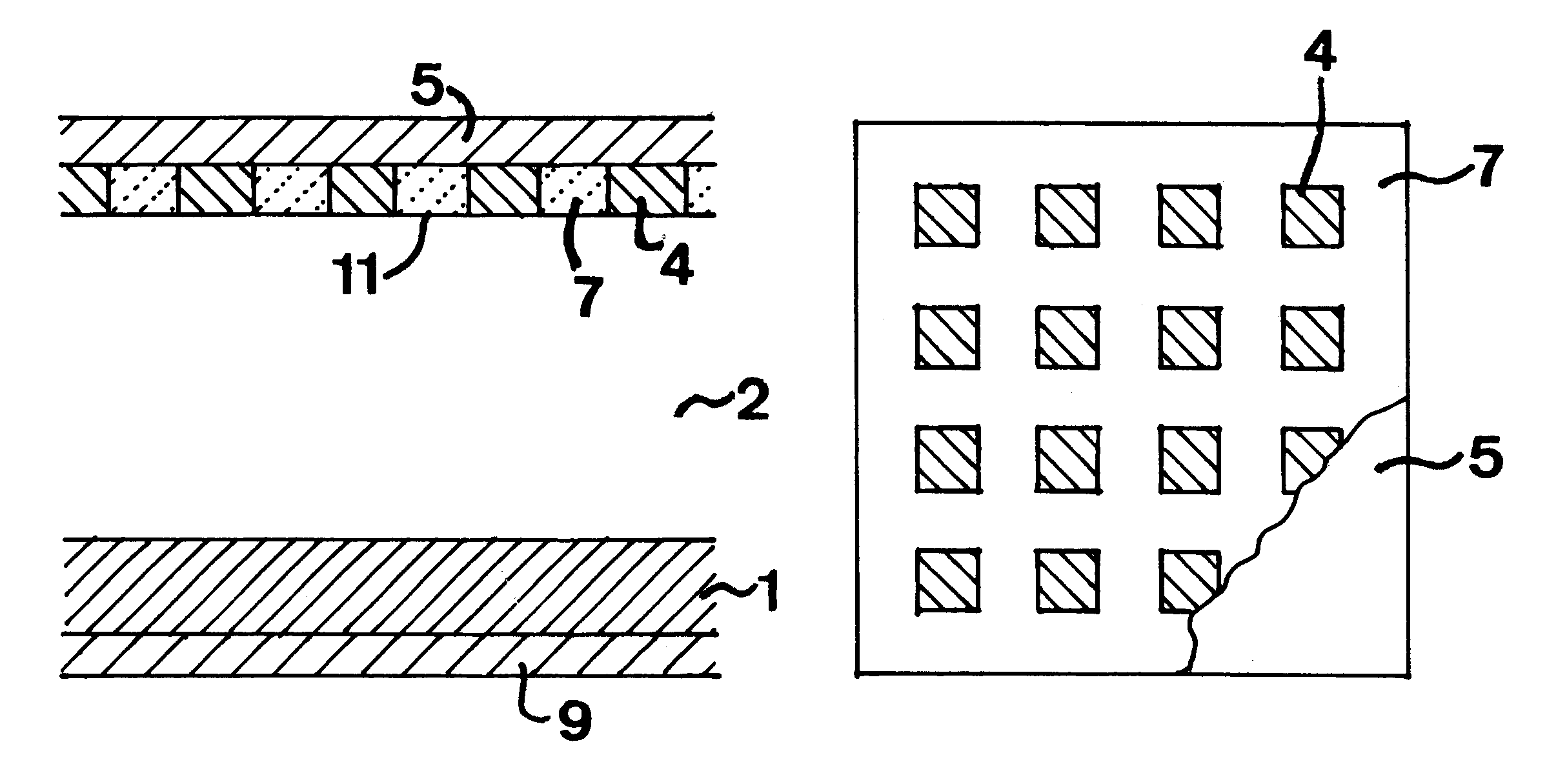
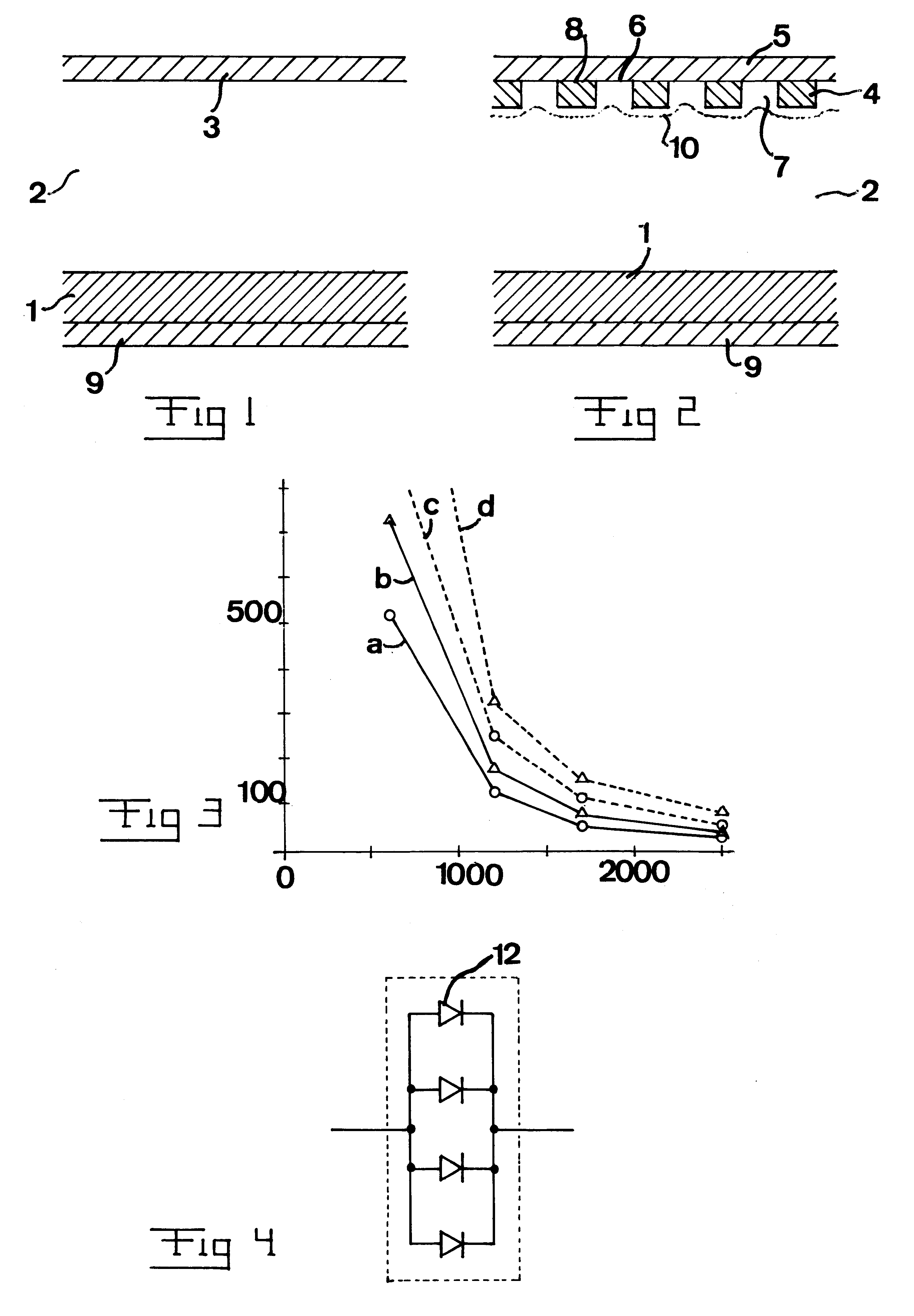
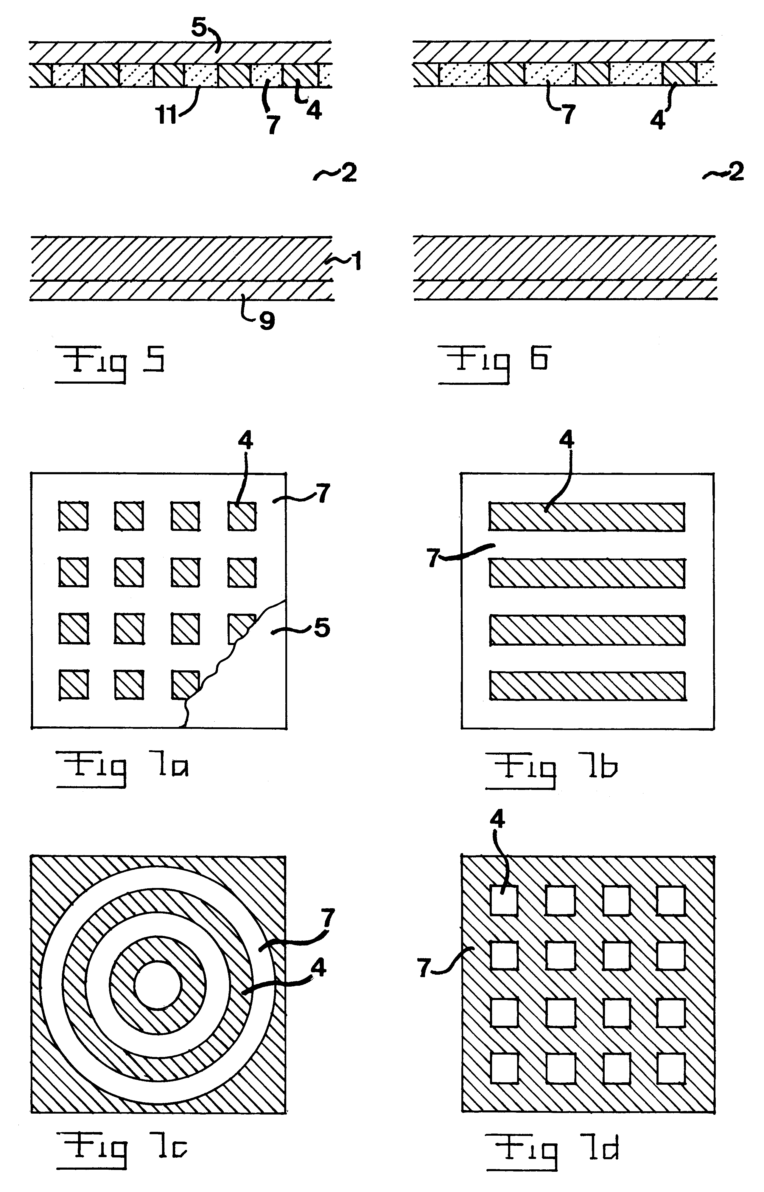
For better understanding the idea of the present invention a conventional Schottky diode is firstly shown in FIG. 1. This Schottky diode of SiC has a highly doped n-type substrate layer 1 and a low doped n-type drift layer 2 on top thereof. A metal layer 3 forming a Schottky contact to the drift layer 2 is applied on top of the latter. If this Schottky diode is made of SiC and for comparatively low blocking voltages, for instance below 2000 V, the drift layer 2 may be made very thin resulting in very low on-state losses, but also in a negative temperature coefficient for the current densities normally of interest. The cross-over point at which the temperature coefficient changes from negative to positive may be lowered by making the drift layer thicker, which will then, as already stated above, substantially increase the on-state losses of the diode.

The present inventors have found that a junction barrier Schottky diode as illustrated in FIG. 2 opens new possibilities to move said c...


PUM


Abstract

A method for controlling the temperature dependence of a junction barrier Schottky diode of a semiconductor material having an energy gap between the valence band and the conduction band exceeding 2 eV provides for doing this when producing the diode by adjusting the on-state resistance of the grid portion of the diode during the production for obtaining a temperature dependence of the operation of the diode adapted to the intended use thereof.

Description

TECHNICAL FIELD OF THE INVENTION AND PRIOR ARTThe present invention relates to a method for controlling the temperature dependence of a junction barrier Schottky diode of a semiconductor material having an energy gap between the valence band and the conduction band exceeding 2 eV. No such method is known today, and the formulation of the goal to obtain such a method constitutes a part of the present invention.A junction barrier Schottky diode is already known through U.S. Pat. No. 6,104,043. That diode is made of SiC, which belongs to the wide band gap materials to which the present invention is directed. The present invention is directed to junction barrier Schottky diodes of all materials having a said energy gap exceeding 2 eV, such as SiC, diamond, AIN etc, but it is particularly directed to such diodes of SiC, so that the present invention will hereinafter be discussed for that material so as to illuminate, but not in any way restrict, the invention and the problems to be solve...

Claims


Application Information

Patent Timeline
Patent Type & Authority Patents(United States)
IPC IPC(8): H01L21/02H01L29/66H01L21/329H01L27/08H01L29/872H01L29/02H01L29/24
CPCH01L27/0814H01L29/872H01L29/66143H01L29/1608
Inventor DAHLQVIST, FANNYLENDENMANN, HEINZHERMANSSON, WILLY
Owner CREE INC
Why Eureka
Try Eureka