Method of fabricating group-III nitride-based semiconductor device

a group-iii nitride-based compound semiconductor and semiconductor technology, which is applied in the direction of semiconductor devices, basic electric elements, electrical equipment, etc., can solve the problems of not being able to achieve the turn-on voltage as well as the brightness of these diodes do not approach the performance level of corresponding devices

Inactive Publication Date: 2003-02-25
NAT UNIV OF SINGAPORE
View PDF17 Cites 91 Cited by
  • Summary
  • Abstract
  • Description
  • Claims
  • Application Information

AI Technical Summary

Problems solved by technology

However, since sapphire is an insulating material and extremely rigid, it is not easy to fabricate a group-III nitride-based semiconductor device on a sapphire substrate.
However, due to the large differences in lattice constant and thermal expansion coefficient between the group-III nitride and silicon, it is really difficult to grow high quality epitaxial layer of group-III nitride-based compound semiconductor on a silicon substrate.
However, the turn-on voltages as well as the brightness of these diodes do not approach the performance levels of corresponding devices grown on sapphire substrates by MOCVD.
At the present time since the physical origin of the composite intermediate layers is unfortunately not very clear, it is truly difficult to theoretically determine or predict the optimal layer thickness of the composite intermediate layers for a special material combination.
However, if the composite intermediate layers are too thin, they may neither effectively accommodate the elastic strain due to the large lattice mismatch between the group-III nitride crystals and the silicon substrate nor provide sufficient amount of seed crystals for the subsequent growth of the group-III nitrides.
On the other hand, if the composite intermediate layers are too thick, they tend to bring about excessive amount of the seed crystals with high orientational fluctuation.

Method used


Image

  • Method of fabricating group-III nitride-based semiconductor device
  • Method of fabricating group-III nitride-based semiconductor device
  • Method of fabricating group-III nitride-based semiconductor device

Examples


example 1

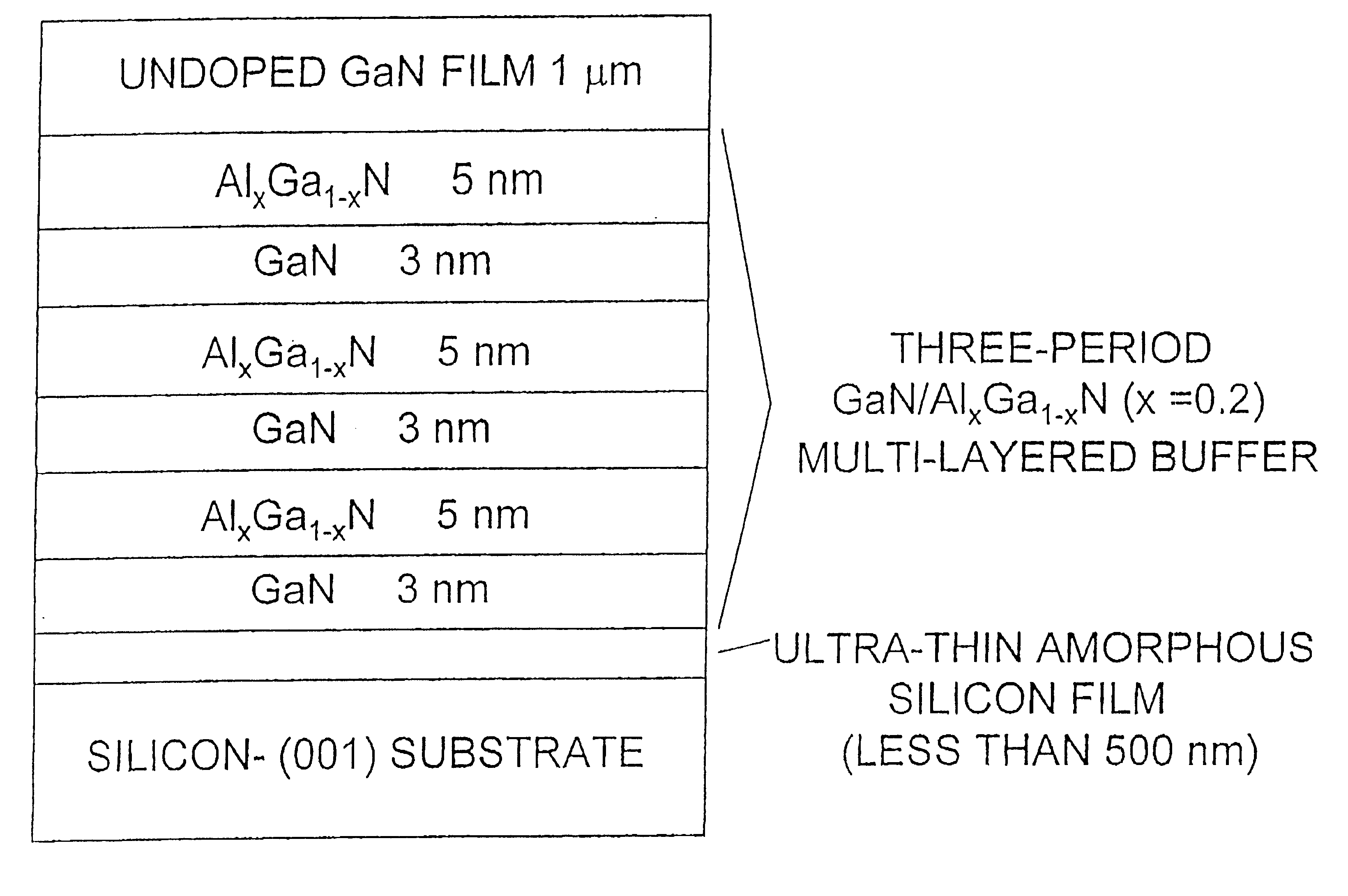
FIG. 3 shows a undoped GAN crystal grown over composite intermediate layers consisting of an ultra-thin (less than 500 nm) amorphous silicon film and a three period GaN / Al.sub.x Ga.sub.1-x N (x=0.2) multi-layered buffer on a silicon (001) substrate. Referring to FIG. 3 after a chemical cleaning process, the silicon (001) substrate is thermal-treated in a MOCVD reactor chamber under hydrogen ambient at a high temperature (preferably over 900.degree. C.) for at least 5 minutes in order to produce a clean, oxide-free surface. The temperature is then reduced to a low temperature (preferably between 400-750.degree. C.), and an ultra-thin (preferably less than 500 nm) amorphous silicon film is deposited on the surface of the above mentioned silicon (001) substrate using hydrogen-diluted silane as a precursor in order to form a "soft" buffer on the silicon substrate. A three period GaN / Al.sub.x Ga.sub.1-x N (x=0.2) multi-layered buffer is then MOCVD-grown on the top of the formed ultra-thi...

example 2

FIG. 6 shows the schematic sectional view of a GaN-based light emitting diode fabricated on a silicon substrate according to Example 2 of the present invention The detailed fabrication process is as follows.

Referring to FIG. 6, after the chemical cleaning process, the n-type silicon (001) substrate on top of which a 150 nm-thick amorphous silicon film was pre-grown by chemical vapor deposition, is heated in a MOCVD reactor chamber under hydrogen ambient at a high temperature (preferably over 900.degree. C.) for at least 5 minutes in order to produce a clean, oxide-free surface. The temperature is then reduced to a lower temperature (preferably between 400-750.degree. C.), and an ultra-thin (preferably less than 500 nm) amorphous silicon film is deposited on the surface of the above mentioned silicon (001) substrate using hydrogen-diluted silane as a precursor in order to form a "soft" buffer on the silicon substrate. A six period GaN / Al.sub.x Ga.sub.1-x N (x=0.2) multi-layered buffe...


PUM

PropertyMeasurementUnit
thicknessaaaaaaaaaa
temperatureaaaaaaaaaa

Abstract

Disclosed are a group-III nitride-based semiconductor device that is grown over the surface of a composite intermediate layers consisting of a thin amorphous silicon film or any stress-relief film or a combination of them and at least one multi-layered buffer on silicon substrate, and a method of fabricating the same device. The intermediate layers that suppress the occurrence of crystal defects and propagation of misfit dislocations induced by the lattice mismatch between the epitaxial layer and substrate, ca n be grown on a part or the entirety of the surface of a silicon (001) or (111) substrate which can be single crystal or coated with a thin amorphous silicon film. Then at least one layer or multiple layers of high quality group-III nitride-based semiconductors are grown over the composite intermediate layers.

Description

1. Field of the InventionThe present invention relates to a method for fabricating group-III nitride-based compound semiconductor devices grown on a substrate consisting of, for example, silicon and, more particularly, to a method for growing epitaxial layers of group-III nitride-based compound semiconductors by means of metalorganic chemical vapor deposition (to be referred to as MOCVD hereinafter).2. Description of the Related ArtTo realize high-efficiency, high-brightness blue and ultraviolet light-emitting diodes and lasers, group-III nitride and related compound semiconductors have been researched and developed in recent years. As a method for growing group-III nitride and related compound semiconductors, MOCVD is currently widely used.In a typical MOCVD process, group-III nitride is grown hetero-epitaxially on a sapphire substrate which is most frequently used at present. However, since sapphire is an insulating material and extremely rigid, it is not easy to fabricate a group...

Claims


Application Information

Patent Timeline
Patent Type & Authority Patents(United States)
IPC IPC(8): H01L21/02H01L21/205H01L33/00
CPCH01L21/02381H01L21/0245H01L21/02458H01L33/007H01L21/0254H01L21/0262H01L21/02507
Inventor ZHANG, XIONGCHUA, SOO JIN
Owner NAT UNIV OF SINGAPORE
Why Eureka
Try Eureka