Efficient current feedback buffer

a current feedback buffer and current current technology, applied in pulse generators, pulse techniques, instruments, etc., can solve the problems of deprived circuits of a part of the limited voltage available and limited minimum input voltage, and achieve greater control of operation and voltage ranges

Inactive Publication Date: 2003-02-25
INFINEON TECH AG
View PDF14 Cites 16 Cited by
  • Summary
  • Abstract
  • Description
  • Claims
  • Application Information

AI Technical Summary

Benefits of technology

The present invention meets these needs by providing a buffered power supply for CMOS devices that uses a current feedback design rather than a voltage feedback design. In one embodiment, a power supply has a first and a second transistor connected in series, the source of the first transistor being connected to the drain of the second transistor, the point of connection being a first point of connection in the circuit. A third transistor has a gate connected to the first point of connection, and the drains of the first and third transistors are then connected to a positive voltage supply. A drain of a fourth transistor is then connected to the source of the third transistor forming a second point of connection. The second point of connection is an output for a voltage to an electronic device, such as a VCO. In this configuration, the third transistor is a principal current source for the VCO, and the fourth transistor is a source follower or buffer for the third transistor. A fifth transistor is then connected at a third point of connection to the sources of the third and fourth transistors, and the source of the fifth transistor is then connected to the negative or return portion of the voltage supply. The first and second transistors provide a negative feedback loop for the power supply. While the embodiments are termed power supplies, it is understood that the embodiments generate a supply and control voltage for a VCO or other device. The current feedback gives the embodiments greater voltage ranges and greater control in operation.

Problems solved by technology

Voltage feedback designs deprive these circuits of part of the limited voltage available.
One significant drawback to this voltage feedback design is that the minimum input voltage is limited by the tail current source 22 of the input differential amplifier and the gate-to-source voltages of the input transistors of the input differential amplifier 20.

Method used


Image

  • Efficient current feedback buffer
  • Efficient current feedback buffer
  • Efficient current feedback buffer

Examples


Embodiment Construction

In the discussion below, transistors are described as CMOS transistors, and in particular as p-channel MOS (PMOS) or n-channel MOS (NMOS) transistors. Those skilled in the art will recognize that the terms p-channel and n-channel might more accurately describe the transistors discussed herein, since these transistors are typically not manufactured by depositing metallic elements, except possibly for external connections. Rather, source and gate regions are doped to either p-type or n-type, indicating whether the channel between source and drain conducts via depletion mode (holes) or enhancement mode (electrons). Nevertheless, the terms PMOS and NMOS are more-commonly used, and are used herein to mean those transistors manufactured by CMOS processes.

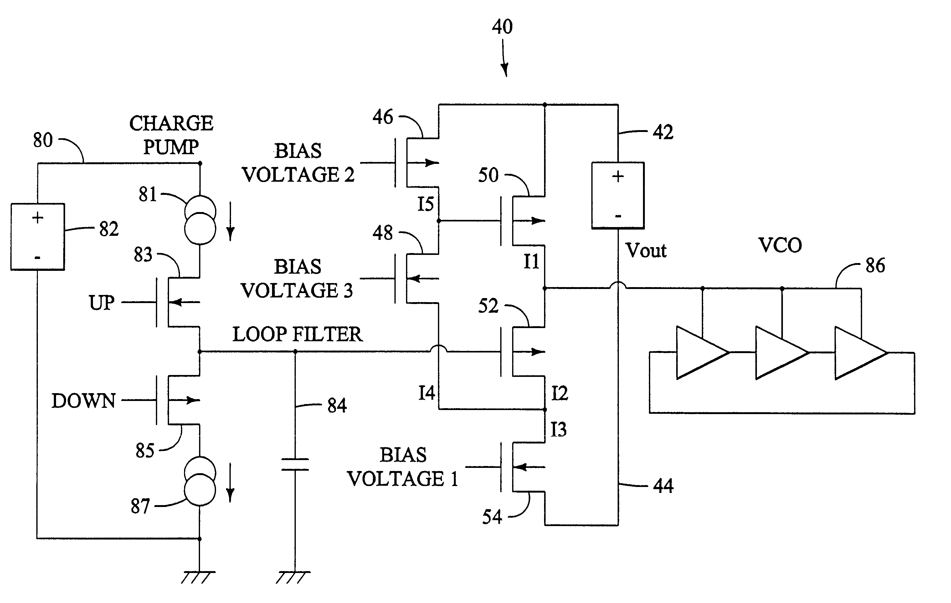
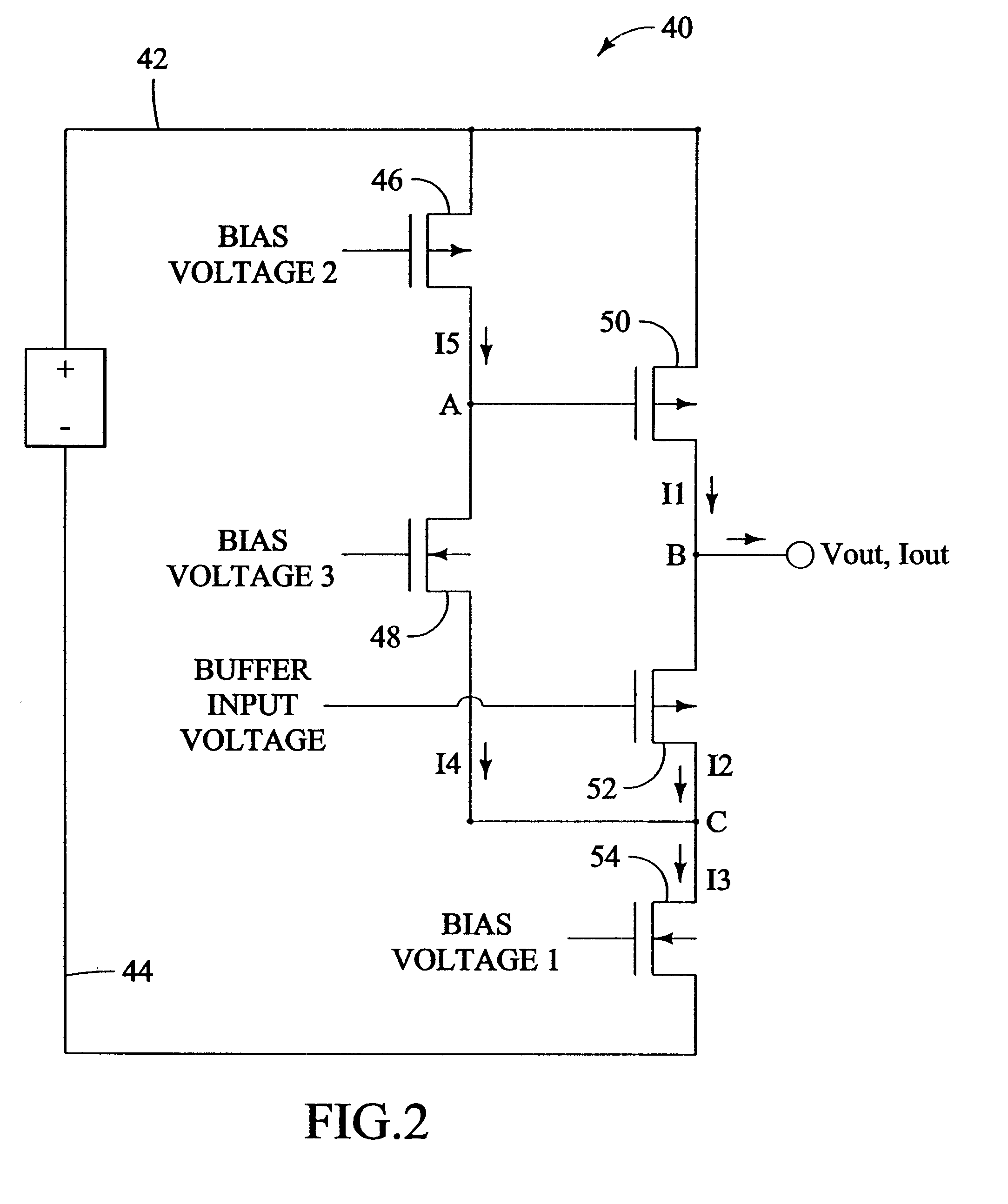
FIG. 2 depicts a first embodiment of a CMOS power supply 40 having current feedback. The power supply 40 includes first, third and fourth transistors 46, 50 and 52, PMOS transistors, and second and fifth transistors 48 and 54, NMOS transi...


PUM


Abstract

An efficient current feedback buffer is revealed. The buffer is useful in power supplies for a number of analog and digital devices, including CMOS voltage controlled ring oscillators, frequency synthesizers, delay locked loops, phase accumulators, and phase locked loops. The power supply and buffer maintains a low impedance output to the load, regulates the voltage output of the supply, and rejects power line noise.

Description

The present invention relates generally to power supplies, and more particularly the present invention relates to buffered current-feedback power supplies useful for integrated circuits made from semiconductors. Power supplies desirably include feedback mechanisms from a load using a power supply, so as to deliver the proper amount of power under the proper conditions. Typically, feedback is achieved by either voltage or current control. Voltage is used because it generally is available with no more effort or circuitry than a voltage divider. Voltage feedback tends to be more useful when there is some possibility that the load will cause a voltage swing, such as a drop in voltage when a heavy load is applied or a spike when a load is suddenly removed.In many small-scale micro-electronics applications, such as very-large scale integration (VLSI), power for power supplies is available only under 5 volts, sometimes as low as 2.5 V or 1.5 V. This is partly to accommodate the ever-smalle...

Claims


Application Information

Patent Timeline
Patent Type & Authority Patents(United States)
IPC IPC(8): G11C5/14H03L7/099H03L7/08H03L7/093H03L7/16H03L7/18
CPCG11C5/147H03L7/1806H03L7/0995H03L7/093
Inventor CYRUSIAN, SASAN
Owner INFINEON TECH AG
Why Eureka
Try Eureka