Image-forming apparatus and method of manufacture therefor
a technology of image-forming apparatus and manufacturing method, which is applied in the manufacture of electric discharge tubes/lamps, tubes with screens, discharge tubes luminescnet screens, etc., can solve the problems of higher cost of manufacturing apparatus, inferior plasma display to crt in image contrast and coloring,
- Summary
- Abstract
- Description
- Claims
- Application Information
AI Technical Summary
Problems solved by technology
Method used
Image

Examples
first embodiment
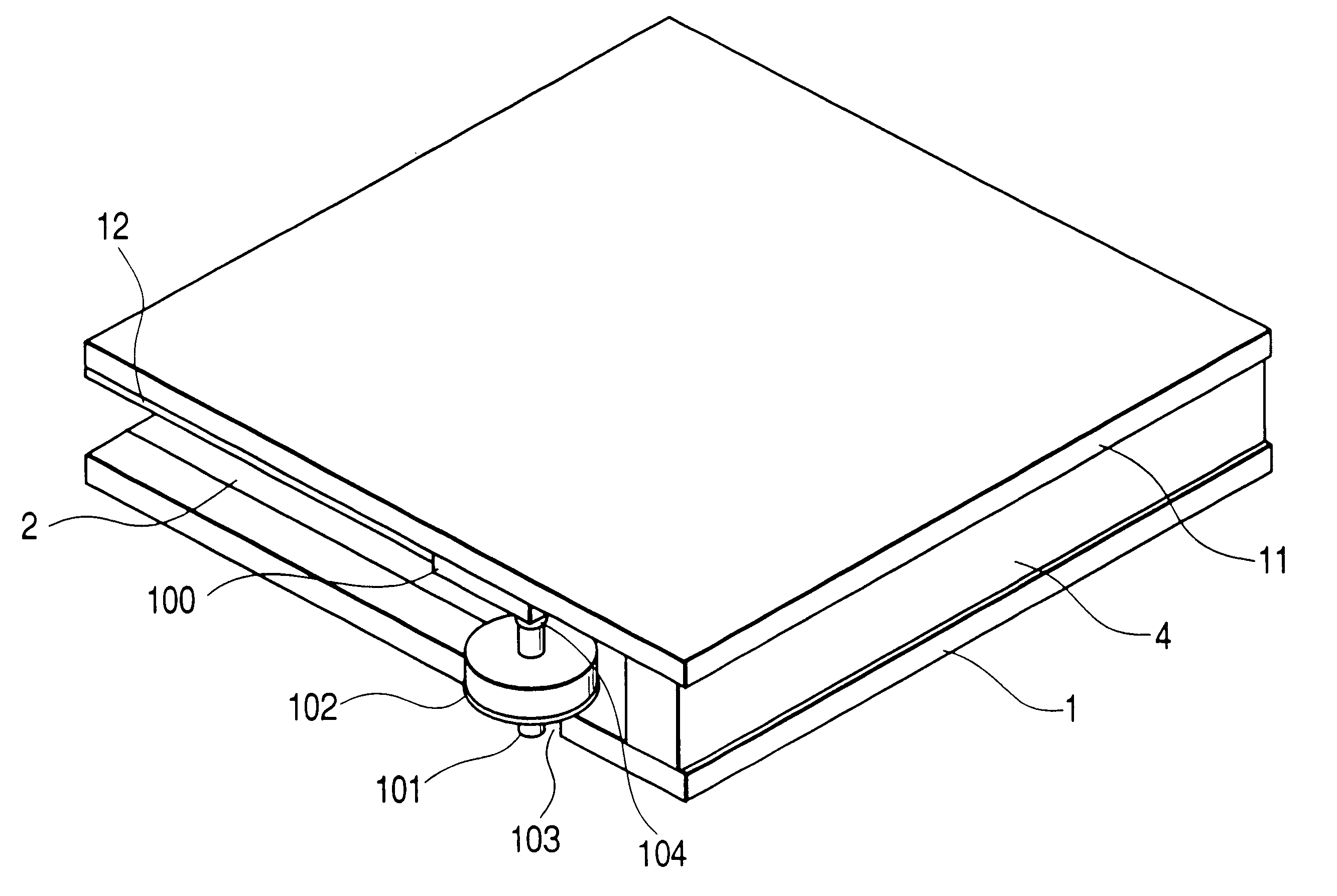
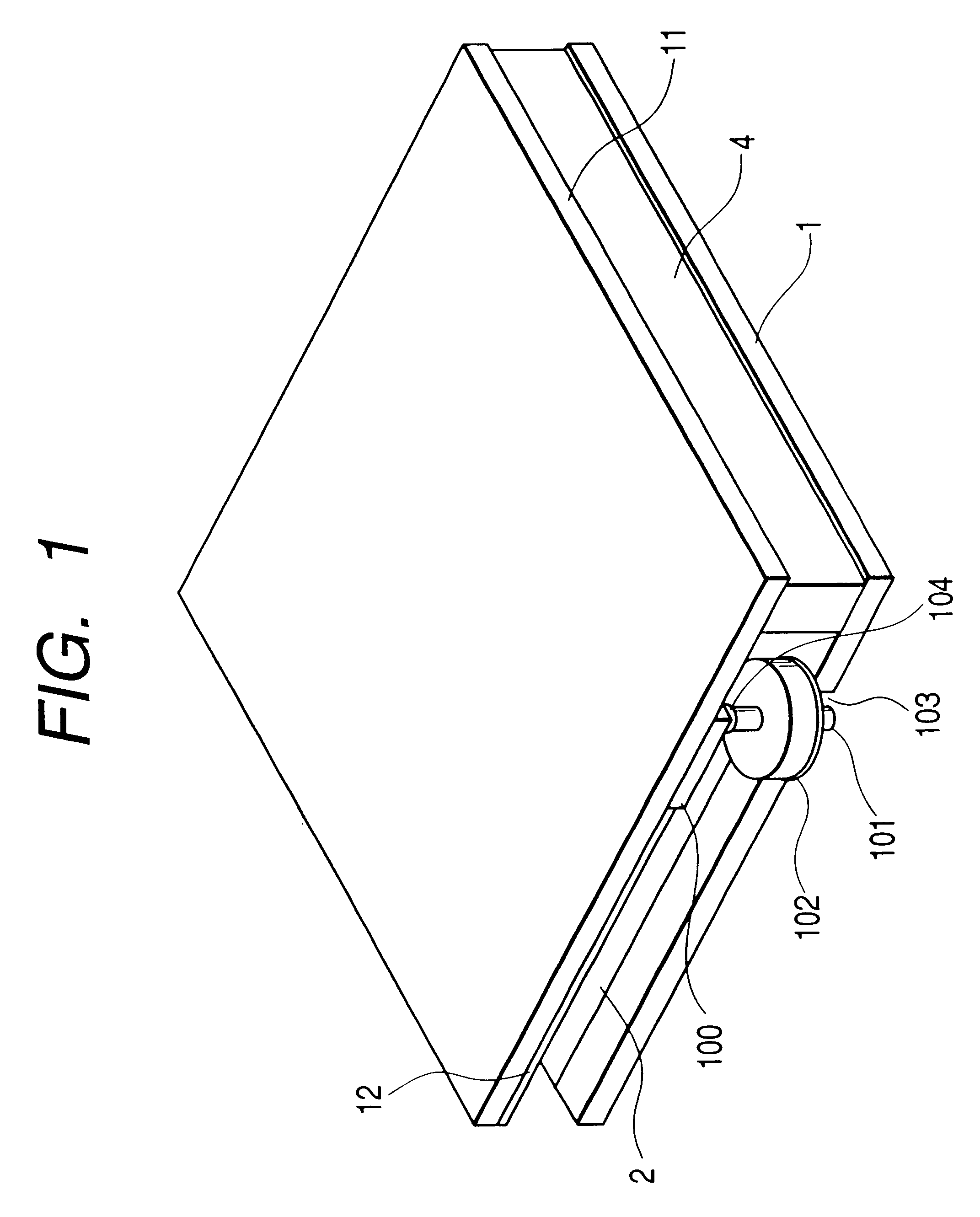
FIG. 1 is a partially broken perspective view which shows around the high voltage connecting structure of an image-forming apparatus in accordance with the present invention. In FIG. 1, a reference numeral 1 designates the rear plate which dually serves as the substrate that forms the electron supply source, and 2, an electron supply source area where a plurality of field emission devices, surface conduction electron-emission devices, or some other electron emission devices are arranged together with the wiring connected with them to serve the purpose. The wiring for use of driving the electron supply source, which is not shown, is led outside the image-forming apparatus and connected with the driving circuit (not shown) of the electron supply source.
A reference numeral 11 designates the face plate that forms an image-forming member; 12, the phosphor that emits light by means of electron emitted from the electron supply source area 2; 100, the lead-out wiring of Ag or the like which...
second embodiment
Now, the description will be made of a second embodiment in accordance with the present invention.
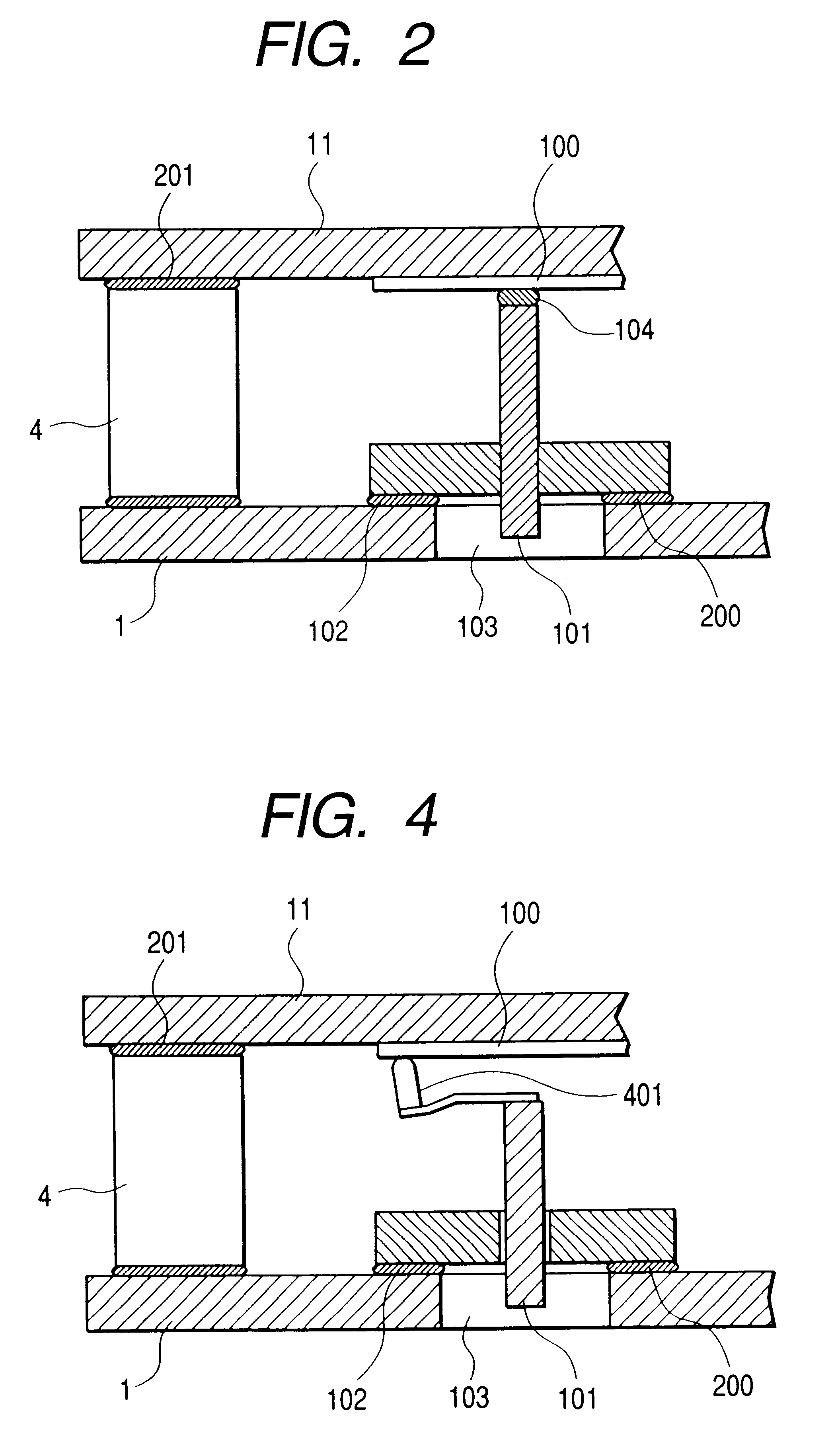
The second embodiment is an example in which a structure that adopts a cantilever spring is arranged for the connecting member. FIG. 4 is a cross-sectional view which shows the anode terminal structure. The structures other than the connecting member are substantially the same as those of the first embodiment. Therefore, the detailed description thereof will be omitted.
In FIG. 4, a reference numeral 401 designates a connecting member which is formed to be a cantilever spring of 2.5 mm long and 0.9 mm wide by etching a stainless steel plate of 0.1 mm thick. Then, Al material is machined to be a semispherical member of 0.5 mm high and 0.9 mm diameter, which Is welded to the leading end of the cantilever spring by use of a laser welder. At the same time, the lead-in terminal 101 is bonded with the base end of the cantilever spring by use of the laser welder. Here, with this bonding, conduc...
third embodiment
Now, with reference to FIGS. 5A and 5B, the description will be made of a third embodiment in accordance with the present invention. FIGS. 5A and 5B are cross-sectional views which illustrate the process in which the anode terminal structure is manufactured.
In FIGS. 5A and 5B, a reference numeral 501 designates a connecting member formed by Ag paste or the like for electrically connecting the lead-out wire 100 with the lead-in terminal which will be described later; 502, the lead-in terminal of 3 mm diameter, having the flat surface where it abuts upon the lead-out wiring 100. With the arrangement of the flat face configuration, the connecting member can be fixed stably on the face plate 11 side. This configuration is preferable because with the wider contact area, a stronger bonding force is obtainable stably.
In this respect, the configuration of the connecting member is not necessarily limited to the flat surface. It may be possible to appropriately select a configuration which is...
PUM
 Abstract
Description
Claims
Application Information
 - R&D
- Intellectual Property
- Life Sciences
- Materials
- Tech Scout
- Unparalleled Data Quality
- Higher Quality Content
- 60% Fewer Hallucinations
Browse by: Latest US Patents, China's latest patents, Technical Efficacy Thesaurus, Application Domain, Technology Topic, Popular Technical Reports.
© 2025 PatSnap. All rights reserved.Legal|Privacy policy|Modern Slavery Act Transparency Statement|Sitemap|About US| Contact US: help@patsnap.com