Semiconductor apparatus, method of fabricating thereof, fabricating apparatus, circuit board, and electronic device

a technology of semiconductor devices and fabrication methods, applied in the direction of semiconductor devices, electrical devices, basic electric elements, etc., can solve the problem of low reliability of semiconductor devices

Inactive Publication Date: 2003-03-11
SEIKO EPSON CORP
View PDF8 Cites 1 Cited by
  • Summary
  • Abstract
  • Description
  • Claims
  • Application Information

AI Technical Summary

Problems solved by technology

The oxide films could deteriorate the adhesion of the resin that seals the lead frame and the semiconductor chip, and could lower the reliability of the semiconductor device.

Method used


Image

  • Semiconductor apparatus, method of fabricating thereof, fabricating apparatus, circuit board, and electronic device
  • Semiconductor apparatus, method of fabricating thereof, fabricating apparatus, circuit board, and electronic device
  • Semiconductor apparatus, method of fabricating thereof, fabricating apparatus, circuit board, and electronic device

Examples


first embodiment

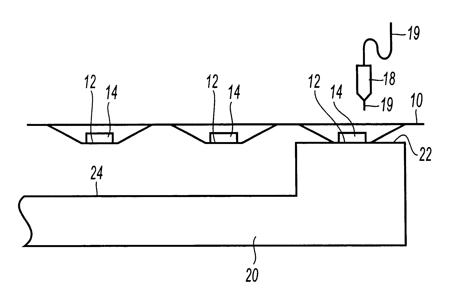
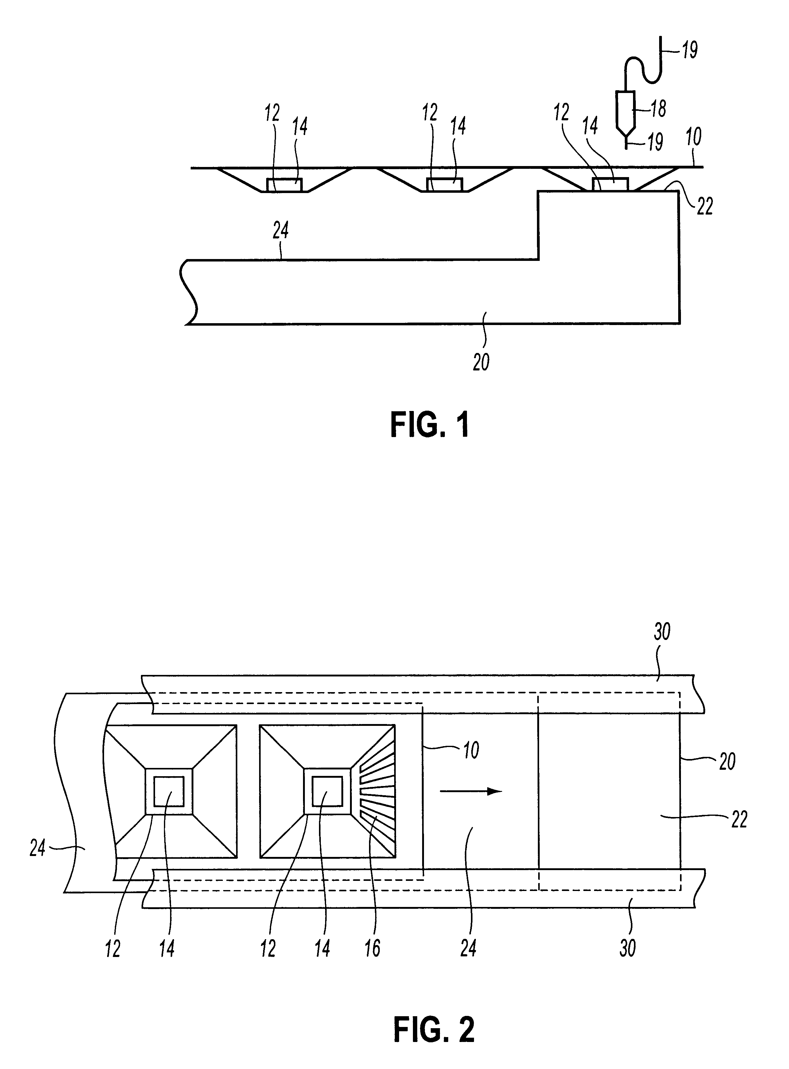
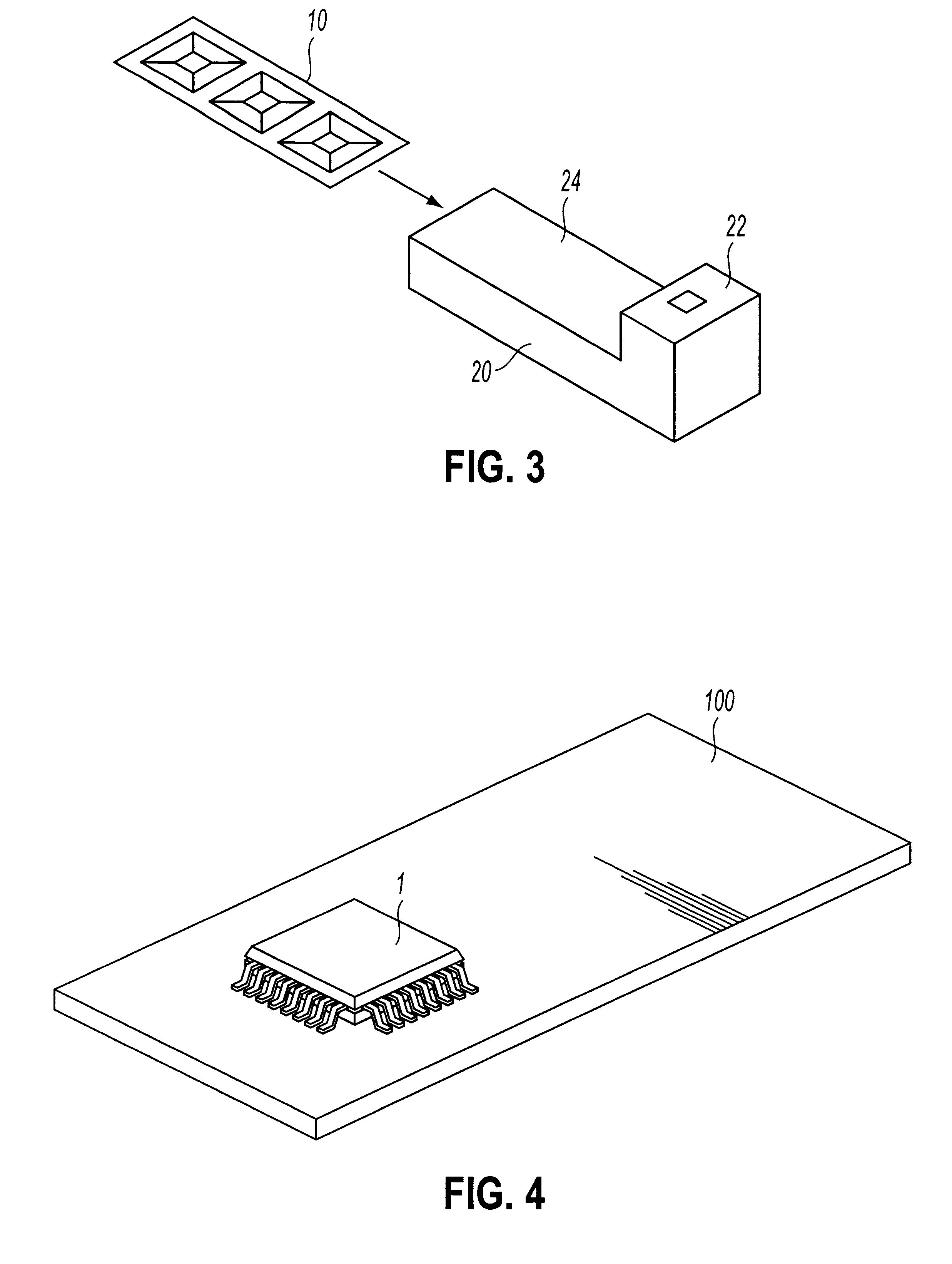
FIGS. 1-3 show a manufacturing method and manufacturing apparatus for a semiconductor device in accordance with the present embodiment, and are a side view, a plan view and a perspective view thereof, respectively.

As shown in FIGS. 1-3, a lead frame 10 is disposed on a bonding apparatus, such that electrodes of semiconductor chips 14 mounted on a plurality of die pads 12 of the lead frame 10 are wire-bonded with leads 16 of the lead frame 10. More specifically, the bonding apparatus includes a bonding stage 22 and a stand-by stage 24, and at least one of the die pads 12 of the lead frame 10 disposed in the bonding stage 22 is wire-bonded.

The lead frame 10 has a plurality of patterns, each of the patterns being formed with a die pad 12 and a plurality of leads 16 (See FIG. 2). In general, from the viewpoint of the productivity, the lead frame 10 having a plurality of patterns, as described above, is processed in a state in which they are connected to each other.

The lead frame 10 is o...


PUM


Abstract

Thermal oxidation of lead frames is provided to thereby improve the adhesion with resin. The method includes the steps of disposing a lead frame having die pads on which semiconductor chips are respectively mounted in a bonding apparatus, and wire-bonding electrodes of the semiconductor chips and leads of the lead frame. The bonding apparatus includes a bonding stage and a stand-by stage. A heat section is provided in the bonding stage. The die pad of the lead frame is disposed in the bonding stage and the remaining die pads are disposed in the stand-by stage. The die pads disposed in the stand-by stage are placed in a non-contact state with the heat section, while the die pad disposed in the bonding stage is brought in contact with the heat section to be heated and wire-bonded.

Description

1. Field of the InventionThe present invention relates to semiconductor apparatuses and fabricating methods, fabricating apparatuses, circuit boards and electronic devices relating to the same.2. Description of Related ArtAs one type of packages for semiconductor devices, QFP (Quad Flat Package) in which a semiconductor chip is mounted on a lead frame is known. More specifically, a semiconductor chip is mounted on a die pad of a lead frame, and electrodes of the semiconductor chip are wire-bonded to leads of the lead frame. Also, the entire semiconductor chip is covered by a resin. It is noted that lead frames are often made from copper.In general, in the wire-bonding process, a lead frame that mounts a plurality of semiconductor chips is transported and the bonding is performed over heat sections that are heated at high temperatures over 200.degree. C. More specifically, the heat sections are provided at a bonding stage where the wire-bonding is performed and a stand-by stage where...

Claims


Application Information

Patent Timeline
Patent Type & Authority Patents(United States)
IPC IPC(8): H01L21/44H01L21/02H01L21/50H01L21/60H01L21/48H01L21/603
CPCH01L24/78H01L24/80H01L24/85H01L24/86H01L2924/01033H01L2224/78H01L2224/85H01L2924/01004H01L2924/01013H01L2924/01029H01L2924/01078H01L2924/01079H01L2924/01082H01L2924/00014H01L2924/01005H01L2924/01006H01L2224/48H01L2224/85205H01L2224/45099H01L2924/00
Inventor MIKAMI, KUNIMITSU
Owner SEIKO EPSON CORP
Why Eureka
Try Eureka