System for generating a reference voltage

a reference voltage and system technology, applied in logic circuits, digital storage, instruments, etc., can solve the problems of reducing the breakdown voltage of the lower threshold device, unable to tolerate the higher external voltage of 2.3-3.6 volts, and low voltage tolerance of the gate transistor operating at voltages of about 1.0 volt or lower, so as to reduce disadvantages and problems, the effect of reducing the disadvantages and problems

Inactive Publication Date: 2003-03-18
GLOBALFOUNDRIES US INC
View PDF3 Cites 16 Cited by
  • Summary
  • Abstract
  • Description
  • Claims
  • Application Information

AI Technical Summary

Benefits of technology

In accordance with the present invention, a system for generating a reference voltage is provided that substantially eliminates or reduces disadvantages and problems associated with conventional systems and methods. In particular, different amounts of resistance are used to maintain the reference voltage at approximately the same voltage level regardless of the external power supply voltage level, and a charge assist circuit is included to more quickly charge the reference voltage.
Technical advantages of one or more embodiments of the present invention include providing an improved system for generating a reference voltage for a voltage level shifter. In a particular embodiment, different amounts of resistance are provided between the reference voltage and ground depending on the mode in which the voltage level shifter is operating. As a result, the difference in voltage levels between an external power supply and the reference voltage is less when the external power supply is lower than when the external power supply is greater. Accordingly, the reference voltage may be maintained at approximately the same voltage level regardless of the mode.
Technical advantages of one or more embodiments of the present invention also include providing a charge assist circuit. In a particular embodiment, the charge assist circuit includes a specified transistor that is shorter than a specified transistor in the reference voltage generator. As a result, more current initially flows through the transistor in the charge assist circuit than through the transistor in the reference voltage generator, resulting in the reference voltage being charged more quickly. In addition, the reference voltage eventually reaches a level at which the charge assist circuit is de-biased, such that the charge assist circuit is essentially placed in a standby mode after the reference voltage is charged. Accordingly, the DC current drawn by the charge assist circuit is minimized when its charging assistance is no longer being used.

Problems solved by technology

Reducing the threshold voltages in this way results in a decrease in the breakdown voltages of the lower threshold devices.
Therefore, these thin-gate transistors operating at voltages of about 1.0 volt or lower have low voltage tolerances.
The internal core circuitry running on the internal source typically uses thin gate oxides and, thus, cannot tolerate the higher external voltages of 2.3-3.6 volts.
However, once internal voltages decreased to the 1 volt range, several of the previously used level translation methodologies could no longer be used.

Method used


Image

  • System for generating a reference voltage
  • System for generating a reference voltage
  • System for generating a reference voltage

Examples


Embodiment Construction

FIGS. 1 through 8, discussed below, and the various embodiments used to describe the principles of the present invention in this patent document are by way of illustration only and should not be construed in any way to limit the scope of the invention. Those skilled in the art will understand that the principles of the present invention may be implemented in any suitably arranged data processing system.

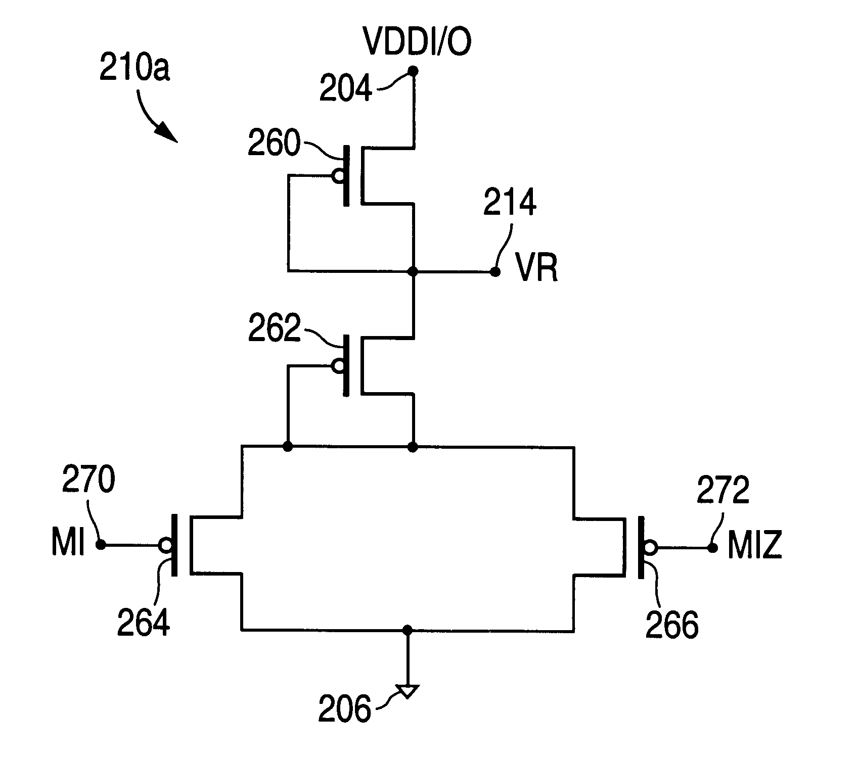
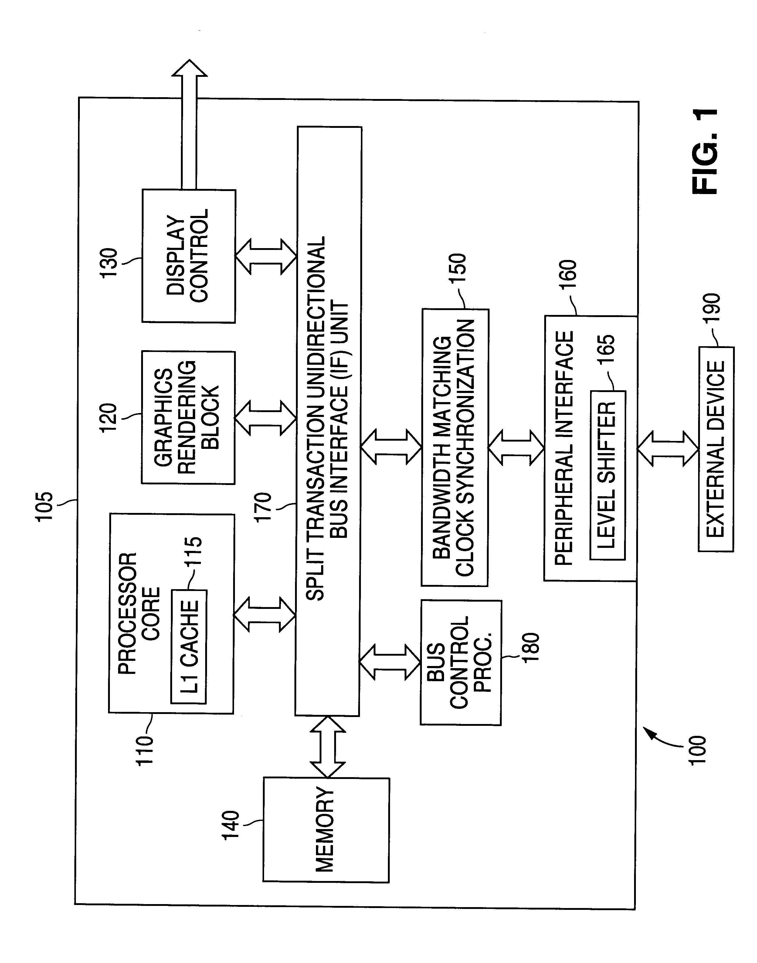
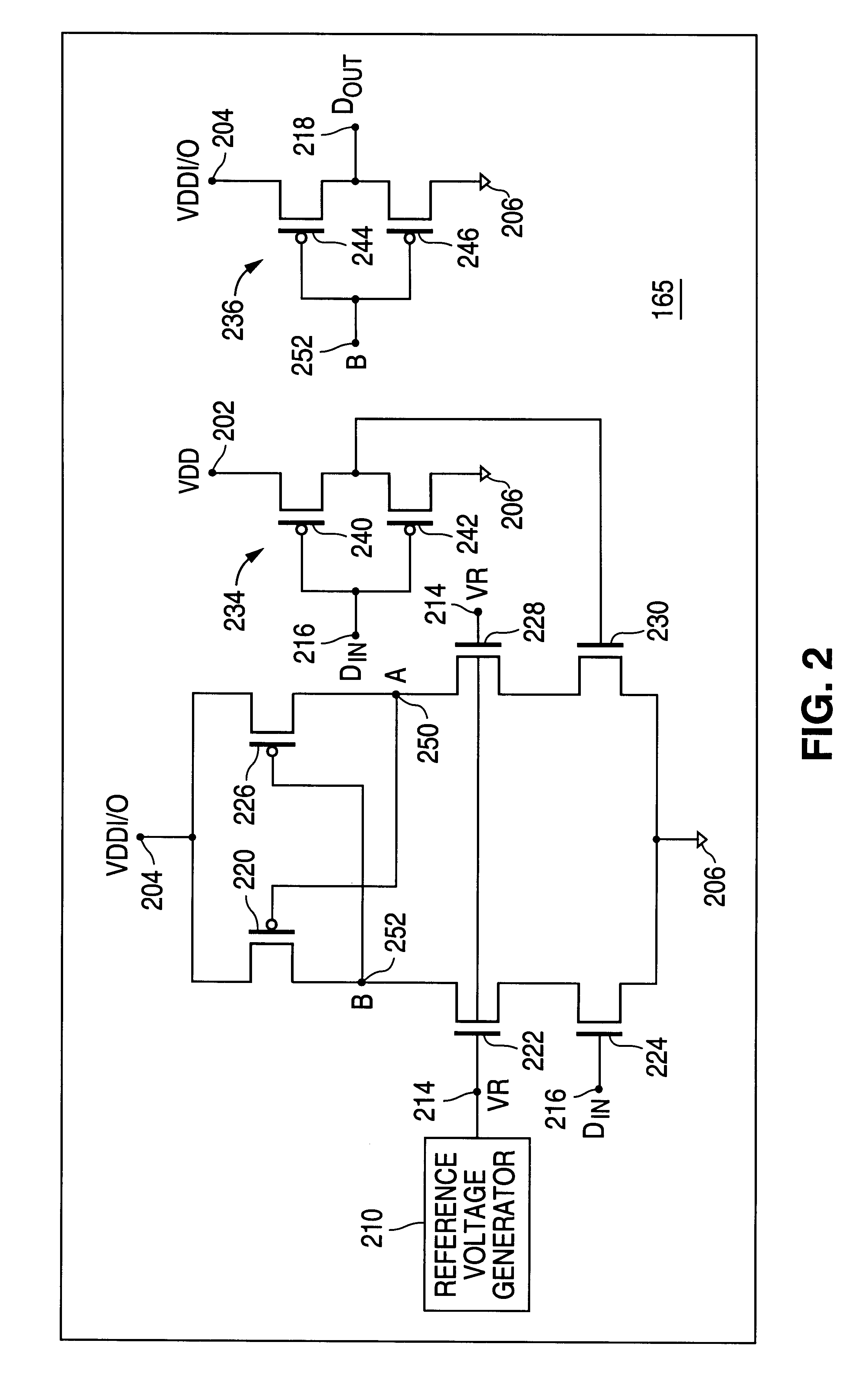
FIG. 1 is a block diagram illustrating a processing system 100 which comprises a system-on-a-chip (SOC) device 105 in accordance with one embodiment of the present invention. The SOC device 105 is a single integrated circuit comprising a processor core 110, an optional graphics rendering block 120, an optional display control circuit 130, a memory 140, a bandwidth-matching clock synchronization interface 150, a peripheral interface 160, a split transaction, unidirectional bus interface (IF) unit 170 (or bus IF unit 170), and a bus control processor 180. The processor core 110 comprise...


PUM


Abstract

A system for generating a reference voltage is provided that includes a first p-type, thick-gate transistor, a second p-type, thick-gate transistor, a third p-type, thick-gate transistor, and a fourth p-type, thick-gate transistor. The first p-type transistor has a source that is coupled to an external power supply, a gate, and a drain that is coupled to the gate. The second p-type transistor has a source that is coupled to the drain of the first p-type transistor, a gate, and a drain that is coupled to the gate. The third p-type transistor has a source that is coupled to the drain of the second p-type transistor, a gate that is operable to receive a mode indicator, and a drain that is coupled to ground. The fourth p-type transistor has a source that is coupled to the drain of the second p-type transistor, a gate that is operable to receive an inverted mode indicator, and a drain that is coupled to ground.

Description

TECHNICAL FIELD OF THE INVENTIONThe present invention is generally directed to integrated circuits and, in particular, to a system for generating a reference voltage.BACKGROUND OF THE INVENTIONIn recent years, there have been great advancements in the speed, power, and complexity of integrated circuits, such as application-specific integrated circuit (ASIC) chips, random access memory (RAM) chips, microprocessor (uP) chips, and the like. These advancements have made possible the development of system-on-a-chip (SOC) devices. A SOC device integrates into a single chip all (or nearly all) of the components of a complex electronic system, such as a wireless receiver (e.g., a cell phone, a television receiver, or the like). SOC devices greatly reduce the size, cost, and power consumption of the overall system.Reductions in power consumption are particularly important in SOC devices. SOC devices are frequently used in portable devices that operate on battery power. Since maximizing batte...

Claims


Application Information

Patent Timeline
Patent Type & Authority Patents(United States)
IPC IPC(8): G11C5/14
CPCG11C5/14
Inventor WERT, JOSEPH D.
Owner GLOBALFOUNDRIES US INC
Why Eureka
Try Eureka