System for fabricating a device on a substrate with a process gas

a technology of process gas and substrate, which is applied in the direction of semiconductor devices, metal material coating processes, coatings, etc., can solve the problems of increasing complexity of microelectronic devices such as integrated circuit chips formed on semiconductor substrate wafers, affecting the integrity of devices, so as to achieve precise control of substrate thermal levels and enhance the effect of uniform film deposition

Inactive Publication Date: 2003-04-08
CVC PRODS
View PDF66 Cites 47 Cited by
  • Summary
  • Abstract
  • Description
  • Claims
  • Application Information

AI Technical Summary

Benefits of technology

Another technical advantage of the present invention is an enhanced capability to combine CVD and PVD reaction chambers along a single hub system. The improved evacuation of residual gas provided by the present invention allows substantially complete removal of residual gas from the reaction chamber and showerhead in a time period that makes throughput of combined PVD and CVD chambers economically feasible.
Another technical advantage of the present invention is the precise control of substrate thermal levels to enhance uniform film deposition across the substrate without deposition on the chuck.
Another technical advantage of the present invention is the reduced evacuation time provided by direct evacuation from the showerhead housing without evacuation of residual gas through the gas dispersion plate. By allowing evacuation of residual gas from both the reaction chamber and the showerhead housing, the present invention reduces the time needed to purge the system in support of wafer handling for further deposition processing.
Another important technical advantage of the present invention is the reduced footprint of the showerhead housing achieved by the side feed of process gas. Reduced footprint can mean substantial savings by allowing room for a greater amount of equipment in the expensive clean rooms used to produce microelectronic devices. Further, feeding process gas to the side of the housing provides improved accessibility for maintenance of the showerhead, and reduced risk of contamination breaking free from flexible hose assemblies.
Another technical advantage of the present invention is the ability to provide a uniform mixture of plural process gases to the reaction chamber without mixing the gases in the housing. The geometric shapes of the openings associated with separate plenums for separate process gas flows enables uniform flow and mixture of the process gases to the reaction chamber. The uniform flow and mixture reduces ring-shaped deposition on the substrate and allows precise control of process gas flows.
Another technical advantage is that games are fed from an enclosed, vented gas box into the showerhead in a safe manner. For instance, all connections can be "dual contained" connections to limit dangers related to gas leakage. Any leakage of toxic gas at these connections can be scavenged by differential pumping and safely removed.

Problems solved by technology

Microelectronic devices, such as integrated circuit (IC) chips formed on a semiconductor substrate wafer, have grown increasing complex over the past several years.
However, the miniaturized circuits are difficult to form.
Minor contamination by impurities and other imperfections have greater and greater effects on the integrity of the devices as the size of circuits within microelectronic devices decrease.
However, it is difficult to manufacture microelectronic devices by combining PVD and CVD processes due to the relatively high pressure of the process gas used in the reaction process chamber for CVD compared to the low pressure used for PVD.
Further, the gases used to support CVD tend to damage substrates if the CVD gases are inadvertently introduced during a PVD process.
Although a deflector plate and showerhead in a conventional CVD system can aid in the relatively uniform distribution of gas across the substrate, this arrangement creates a number of difficulties in the commercial production of microelectronic devices on a substrate wafer.
This can increase the amount of precursor gas needed for deposition of a given film.
Further, the inlet and associated fittings increase the difficulty of showerhead maintenance, and the likelihood of contamination during CVD processing.
These hoses impede access to the showerhead housing, and can include particulate contaminates that can break free during CVD processing to introduce contaminants to the substrate.
Another difficulty associated with conventional CVD systems relates to system throughput.
The low conductance of the reaction chamber and showerhead dispersion plate openings tends to increase the time needed to evacuate the reaction chamber since the evacuation pump has to draw residual process gas through the openings for evacuation of the showerhead housing.
In low-conductance systems, baffles associated with the reaction chamber also impede evacuation of residual gas.
Further, even with an extensive evacuation time, residual gas typically remains in the precursor delivery line, the showerhead housing and the reaction chamber, resulting in plating of material from the precursor on the wafer handling system, such as the wafer chuck, when the residual gas decomposes, and eventual contamination of the system.
Increased evacuation time can decrease the presence of residual gas, but even extensive evacuation times generally cannot eliminate the residual gas from the showerhead and reaction chamber before transfer of the substrate wafer through the hub.
Another difficulty of conventional CVD systems results from CVD processes that use two or more gases to deposit a material on a substrate.
For instance, a precursor and reducing gas chemically support deposition of a material on a substrate, but are chemically incompatible if mixed before delivery to the substrate.
If the precursor and reducing gas are mixed in the delivery line or showerhead housing before flowing to the reaction chamber, they will generate particles that cause blockage of the gas delivery system and that can cause undesired composition of the film material.
The increased flow resistance decreases system throughput by increasing pumping and purging cycle times and can cause condensation of pressure-sensitive precursor vapor.
Further, the multi-zone showerhead design is difficult to manufacture and inflexible with respect to its use with various combinations of gases, flow rates and reactor geometries.
Another difficulty associated with CVD relates to the deposition of the material from the precursor gas to the reaction chamber walls and to the chuck-that supports the substrate in the reaction chamber.
CVD of a copper film presents increased difficulty due to the narrow range of conditions in which the copper precursor is stable.
For instance, one typical copper precursor will decompose at temperatures above 100 C, and will condense at temperatures below 50 C. Thus, over a series of CVD depositions, a reaction chamber and chuck used for copper deposition tends to have a residual film of copper build, which can interfere with subsequent depositions.

Method used


Image

  • System for fabricating a device on a substrate with a process gas
  • System for fabricating a device on a substrate with a process gas
  • System for fabricating a device on a substrate with a process gas

Examples


Embodiment Construction

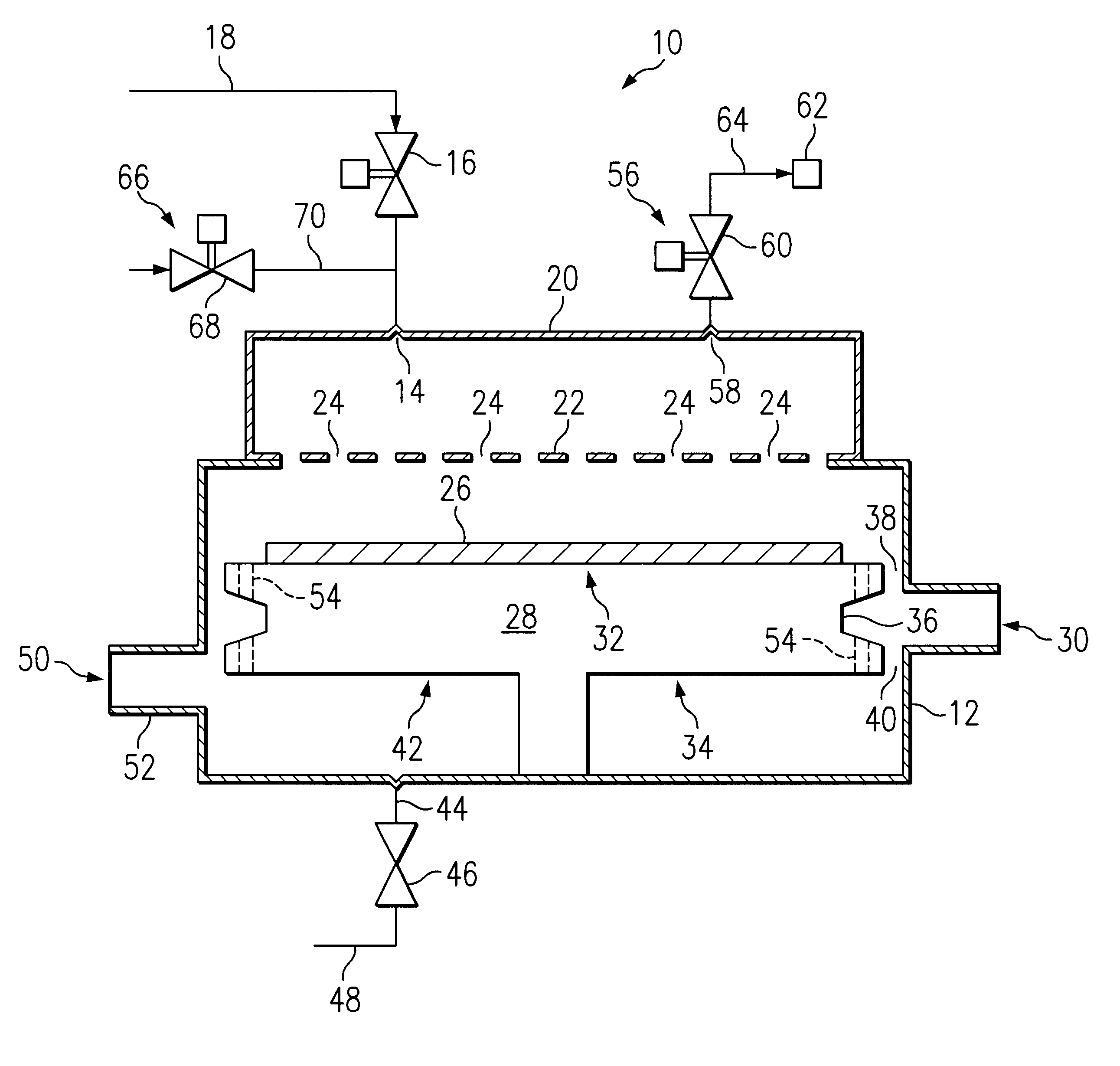
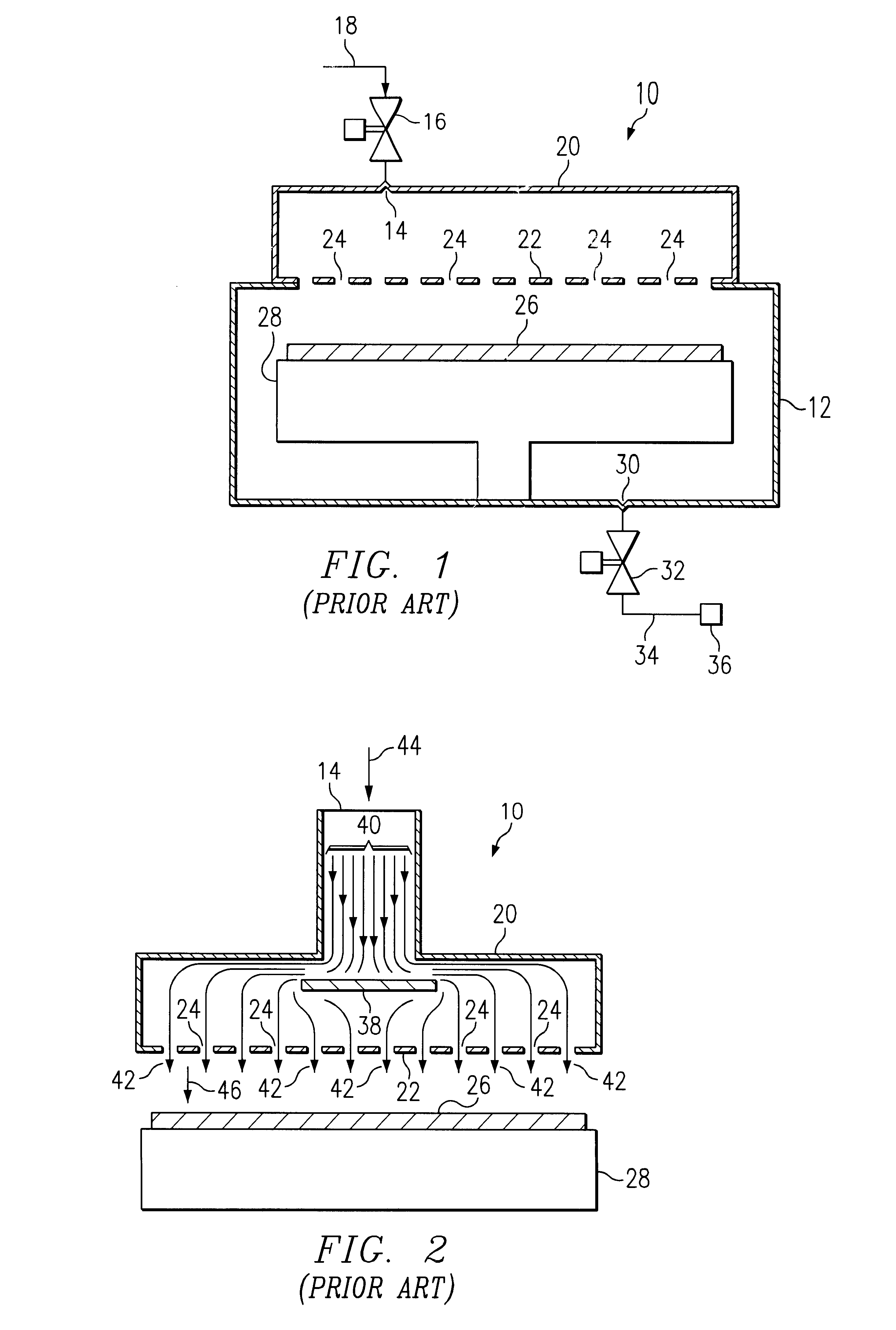
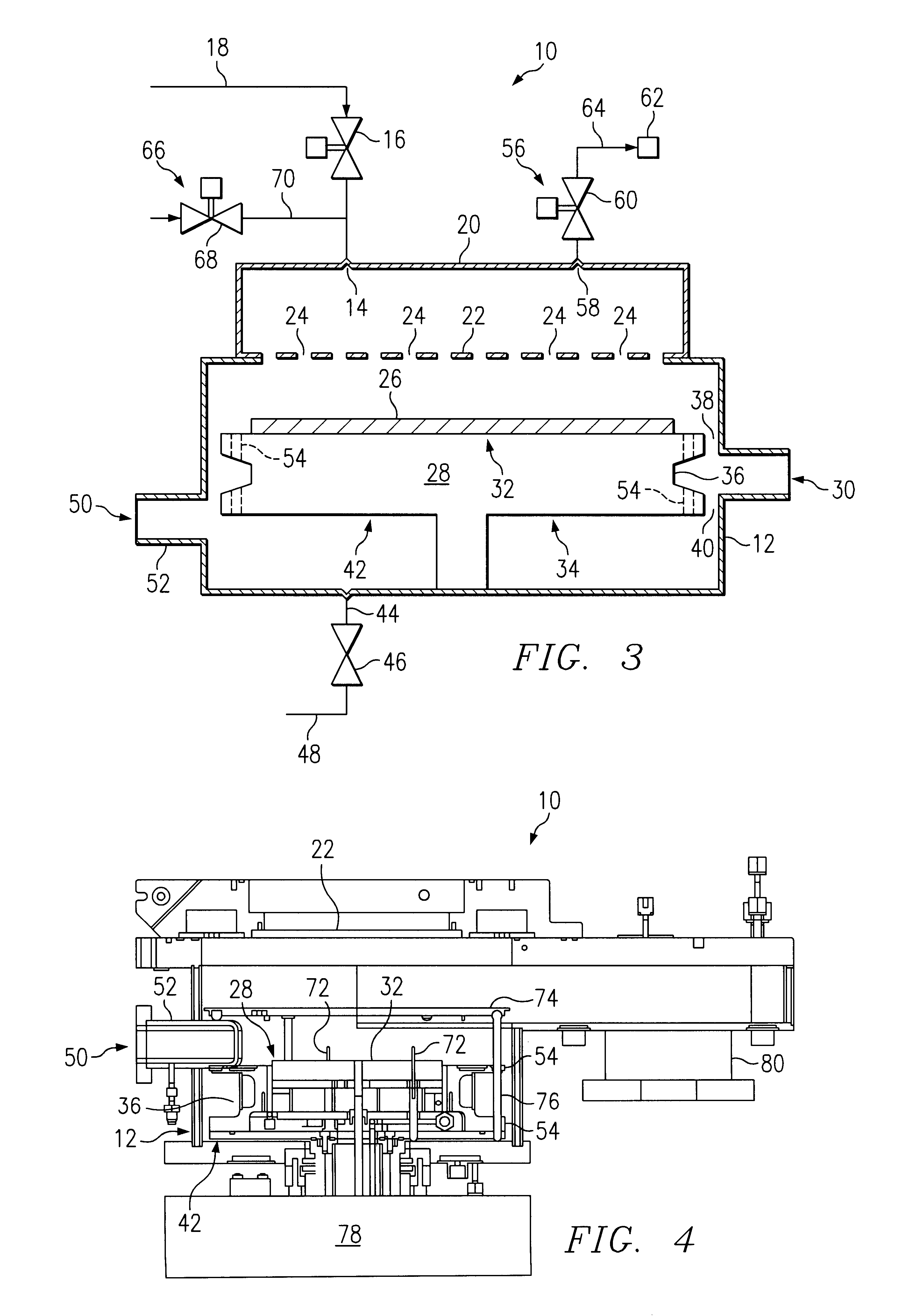
CVD provides many advantages as a technique for the deposition of uniform thin film materials on a substrate for the formation of microelectronic devices. Under properly controlled conditions, CVD allows the deposition of uniform and precise thicknesses of a number of materials. However, the deposition of quality material films by CVD requires a uniform flow of CVD process gases in a clean environment with minimal contamination by particulate and other impurities.

For instance, CVD of copper is accomplished by flow of a copper-carrying precursor, such as CUPRASELECT.TM., over the substrate at predetermined temperature and pressure conditions. The precursor decomposes, releasing the copper material to deposit on the substrate. By maintaining a uniform flow of the precursor over the substrate, a uniform copper film is deposited on the substrate. However, once the deposition of the material film is complete, residual precursor present in the CVD system can result in undesired deposition...


PUM

PropertyMeasurementUnit
circumferenceaaaaaaaaaa
conductanceaaaaaaaaaa
temperatureaaaaaaaaaa

Abstract

A method and system for fabricating a device on a substrate with a process gas, such as with chemical vapor deposition. A reaction chamber and support chuck cooperate to form a low conductance configuration for axisymetric process gas flow over the substrate and to form a high conductance configuration for enhanced evacuation of residual process gas from the reaction chamber upon completion of the process. A dual conductance chuck has an indented region that aligns with the exhaust port of the reaction chamber to restrict process gas flow in the low conductance configuration, and that moves distal a showerhead and the exhaust port to provide reduced restriction of process gas flow for reaction chamber evacuation. The chuck includes thermal control for enhancing film deposition on the substrate and for reducing residual film deposition on the chuck. An evacuation opening in the housing provides independent evacuation of residual gas from the housing. The present invention enhance throughput of device formation by reducing purge and process cycle times.

Description

TECHNICAL FIELD OF THE INVENTIONThis invention relates in general to the field of semiconductor device fabrication, and more particularly to a method and system for dispensing process gas for fabricating a device on a substrate.BACKGROUND OF THE INVENTIONMicroelectronic devices, such as integrated circuit (IC) chips formed on a semiconductor substrate wafer, have grown increasing complex over the past several years. By miniaturizing the circuits of the microelectronic devices, industry has achieved significant performance improvements in terms of increased processing speed and decreased footprint. However, the miniaturized circuits are difficult to form. Minor contamination by impurities and other imperfections have greater and greater effects on the integrity of the devices as the size of circuits within microelectronic devices decrease. As industry transitions from the present 0.25 micron circuit devices to devices having smaller circuits, such as 0.18 and 0.13 microns, device for...

Claims


Application Information

Patent Timeline
Patent Type & Authority Patents(United States)
IPC IPC(8): C23C16/458C23C16/44C23C16/455
CPCC23C16/4408C23C16/4412C23C16/45521C23C16/45589C23C16/4585C23C16/45565Y10S438/905
Inventor OMSTEAD, THOMAS R.WONGSENAKHUM, PANYAMESSNER, WILLIAM J.NAGY, EDWARD J.STARKS, WILLIAM EMOSLEHI, MEHRDAD M.
Owner CVC PRODS
Why Eureka
Try Eureka