Substrate processing apparatus and processing method by use of the apparatus

a technology of substrate and processing method, which is applied in the field of developing apparatus, can solve the problems of large amount of developing solution, high cost of treating waster water, and difficulty in achieving uniform development, and achieve the effect of improving the quality of the substrate and reducing the cost of treatmen

Inactive Publication Date: 2003-04-22
TOSHIBA MEMORY CORP
View PDF14 Cites 76 Cited by
  • Summary
  • Abstract
  • Description
  • Claims
  • Application Information

AI Technical Summary

Problems solved by technology

However, the dip method and the spray method have problems.
They require a large amount of developing solution and much cost for treating waster water.
The paddle method, however, has a problem of nonuniform development.
However, the conventional scan-development mentioned above is accompanied by such a problem that the pattern size finally obtained differs from the predetermined pattern size due to uneven density of the pattern.
Due to the uneven density of the pattern, a pattern cannot be obtained with high accuracy.
Hence, the pattern cannot be obtained with high accuracy.

Method used


Image

  • Substrate processing apparatus and processing method by use of the apparatus
  • Substrate processing apparatus and processing method by use of the apparatus
  • Substrate processing apparatus and processing method by use of the apparatus

Examples


second embodiment

In the first place, an anti-reflection film was formed on a disk-form Si wafer of 30 cm diameter and further a chemically amplified photoresist film was formed, which had a sensitivity to light of 193 nm wavelength. Subsequently, light of 193 nm wavelength was selectively exposed to the Si wafer surface via a light-exposure mask. As a result, an acid was generated from the photoresist film. Furthermore, the Si wafer was heated at 140.degree. C. for 60 seconds to disperse the acid. In this manner, a latent image was formed.

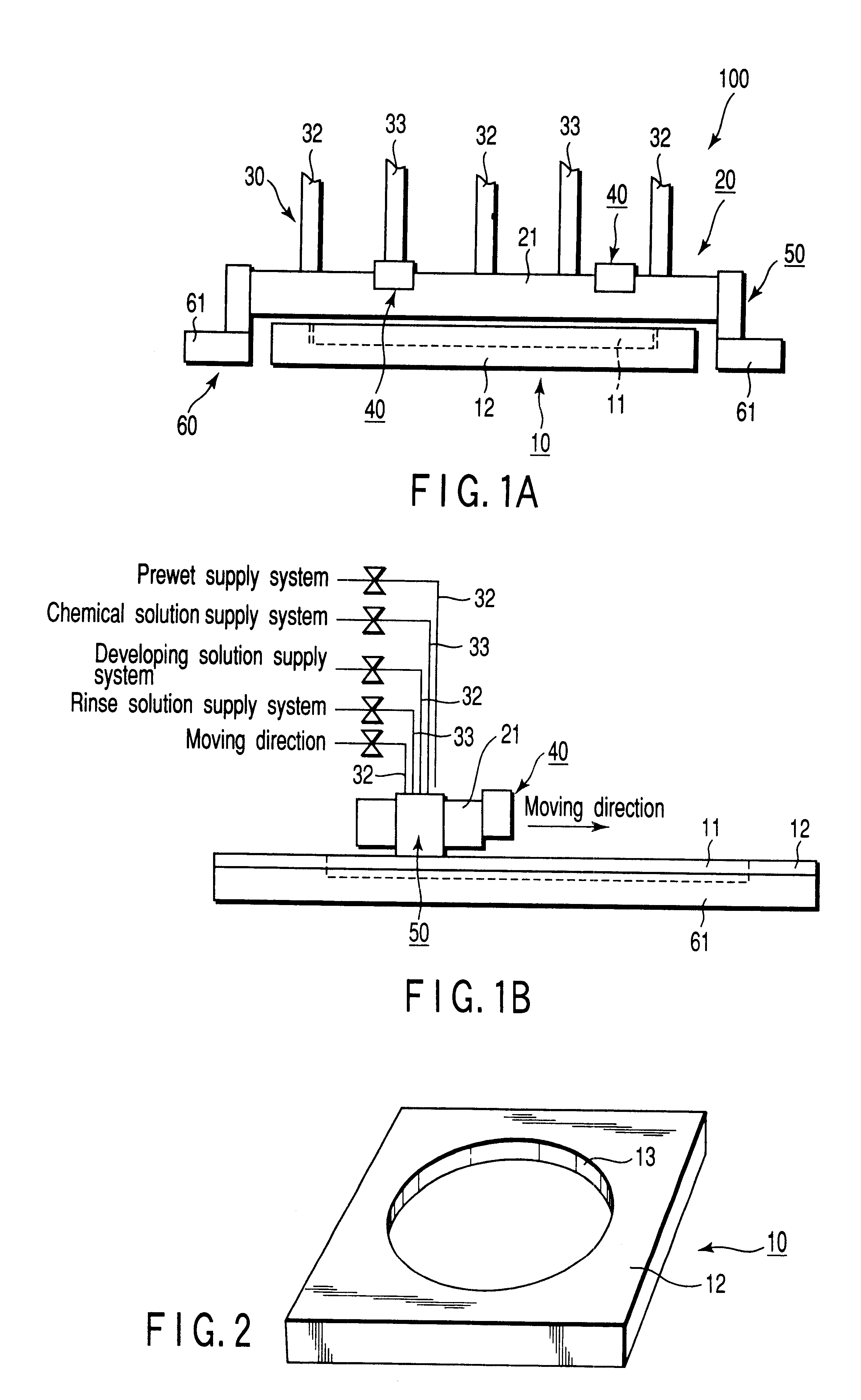
The Si wafer 11 was then housed in the depressed portion 13 of the substrate holder 12.

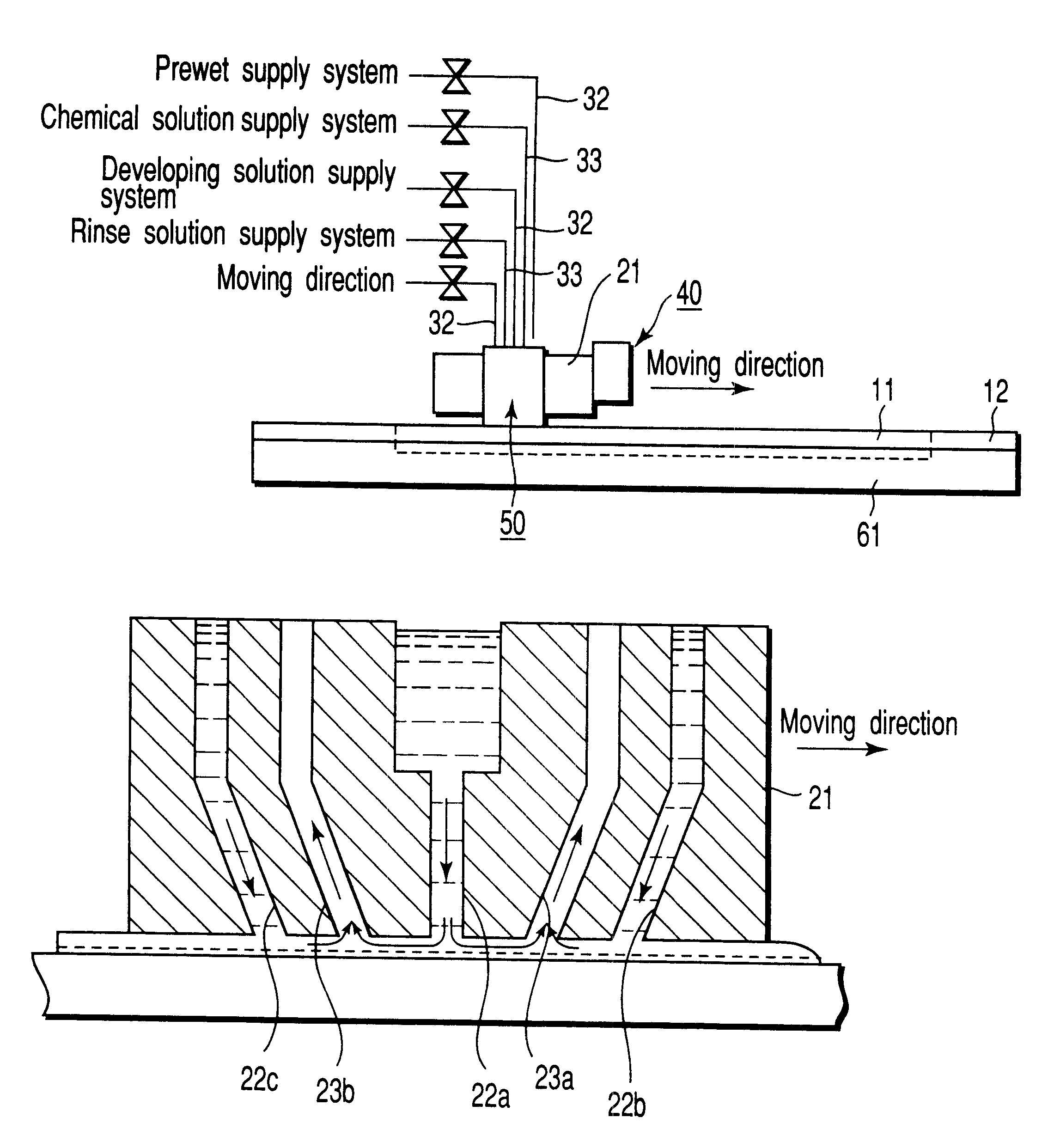
As shown in FIG. 5A, the scan nozzle 21 was arranged on the substrate holder 12 at an interval of about 50 .mu.m from one end portion A of the substrate holder 12. Subsequently, the developing solution, the prewet solution, and the rinse solution were allowed to discharge onto the substrate holder 12 from the developing solution outlet 22a, the prewet solution outlet 22b, and the...

third embodiment

An Example in which the developing device of the aforementioned example is applied to manufacturing of a photo mask substrate will be explained.

To a Cr mask coated with a chemically amplified positive resist (500 nm thick), a 1 GDRAM pattern having a line-and-space under a 0.15 .mu.m rule was drawn by an electron beam drawing device at an acceleration voltage of 50 keV. After the pattern was drawn, baking was performed for 15 minutes at 110.degree. C.

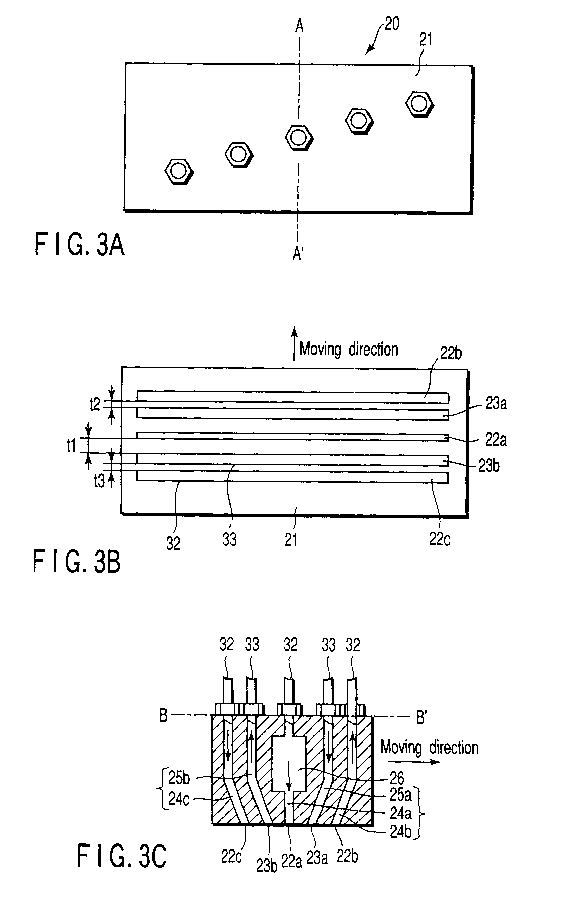
Subsequently, a substrate was mounted on the developing apparatus of this embodiment, and the scan nozzle was moved from one end A toward the other end B (opposite to the end A) at a constant speed. The development was performed in this manner. The moving speed was 11 mm / minute. The interval between the developing solution outlet 22a and the chemical solution inlet 23a was 5 mm. The same interval was present on the other side of the developing solution outlet 22a. In addition, the width of the developing solution outlet 22a was 1 mm. Fr...

fourth embodiment

FIG. 7 shows a schematic structure of a substrate processing portion of the developing apparatus according to the fourth embodiment of the present invention. In FIG. 7, like reference numerals are used to designate like structural elements corresponding to those like in FIGS. 3A to 3D and FIG. 4 and any further explanation is omitted for brevity's sake.

In this embodiment, the developing solution outlet 22a positioned between the port 22b and the port 22c is arranged except the middle point of them. In the case of this example, the developing solution outlet 22a is positioned in the front half to the middle point in the moving direction. The rinse solution is discharged from both the port 22b and the port 22c.

As shown in FIG. 7, a wafer 72 is mounted on the surface of the substrate holder 13. The substrate holder 13 is formed of a wafer holding tool 75 having the same diameter as that of the wafer and a liftable auxiliary board 78 surrounding the wafer holding tool 75 and the wafer 7...


PUM

PropertyMeasurementUnit
lengthaaaaaaaaaa
lengthaaaaaaaaaa
widthaaaaaaaaaa

Abstract

An apparatus for processing a substrate comprising a substrate holding mechanism for holding the substrate substantially horizontally, a chemical solution discharge/suction mechanism having a chemical solution discharge/suction portion which has a chemical solution outlet for discharging a chemical solution onto the substrate and chemical solution inlets for sucking up the chemical solution present on the substrate, and a chemical solution supply/suction system for supplying the chemical solution to the chemical solution discharge/suction mechanism simultaneously with sucking the chemical solution by the chemical solution supply/suction mechanism.

Description

This application is based upon and claims the benefit of priority from the prior Japanese Patent Applications No. 2000-388357, filed Dec. 21, 2000; and No. 2001-304016, filed Sep. 28, 2001, the entire contents of both of which are incorporated herein by reference.1. Field of the InventionThe present invention relates to a substrate processing apparatus and a substrate processing method for use in the steps of manufacturing semiconductor devices, photomasks, liquid crystal displays, etc. The present invention particularly relates to a developing apparatus and a developing method by use of the developing apparatus for developing a substrate coated with a photoresist and exposed to light via a predetermined pattern.2. Description of the Related ArtIn the steps of manufacturing semiconductor devices and liquid crystal displays, a photoetching process is repeatedly applied to a substrate. In the photoetching process, a photoresist is applied to a substrate, and the photoresist-coated sub...

Claims


Application Information

Patent Timeline
Patent Type & Authority Patents(United States)
IPC IPC(8): G03D5/00G03F7/30G03F7/40H01L21/027H01L21/304H01L21/306
CPCG03D5/003G03F7/30
Inventor SAKURAI, HIDEAKIITOH, MASAMITSUITO, SHINICHI
Owner TOSHIBA MEMORY CORP
Why Eureka
Try Eureka