Flip-chip assembly of semiconductor devices using adhesives

a technology of semiconductor devices and adhesives, applied in the direction of contact member assembly/disassembly, electrical apparatus, solid-state devices, etc., can solve the problems of inconvenient assembly process, inconvenient use, and inability to meet the requirements of the assembly process, so as to achieve a simple, reliable and cost-effective assembly process.

Inactive Publication Date: 2003-04-29
INTERUNIVERSITAIR MICRO ELECTRONICS CENT (IMEC VZW)
View PDF10 Cites 60 Cited by
  • Summary
  • Abstract
  • Description
  • Claims
  • Application Information

AI Technical Summary

Benefits of technology

An aim of the present invention is to offer, in comparison to the state of the art, a simplified, reliable and cost-effective assembly process.

Problems solved by technology

Therefore the technologies, applied in these assemblies, are often limited to well established and qualified technologies like reflow and wave soldering of standard SMT (surface-mount-technologies) and through-hole components.
The author reported non-consistent electrical stability or even mechanical failure of the adhesive junctions.

Method used


Image

  • Flip-chip assembly of semiconductor devices using adhesives
  • Flip-chip assembly of semiconductor devices using adhesives
  • Flip-chip assembly of semiconductor devices using adhesives

Examples


first embodiment

In the present invention, illustrated in FIGS. 4A-4F, an assembly process for flip-chip mounting of devices to a substrate is disclosed, comprising the steps of:

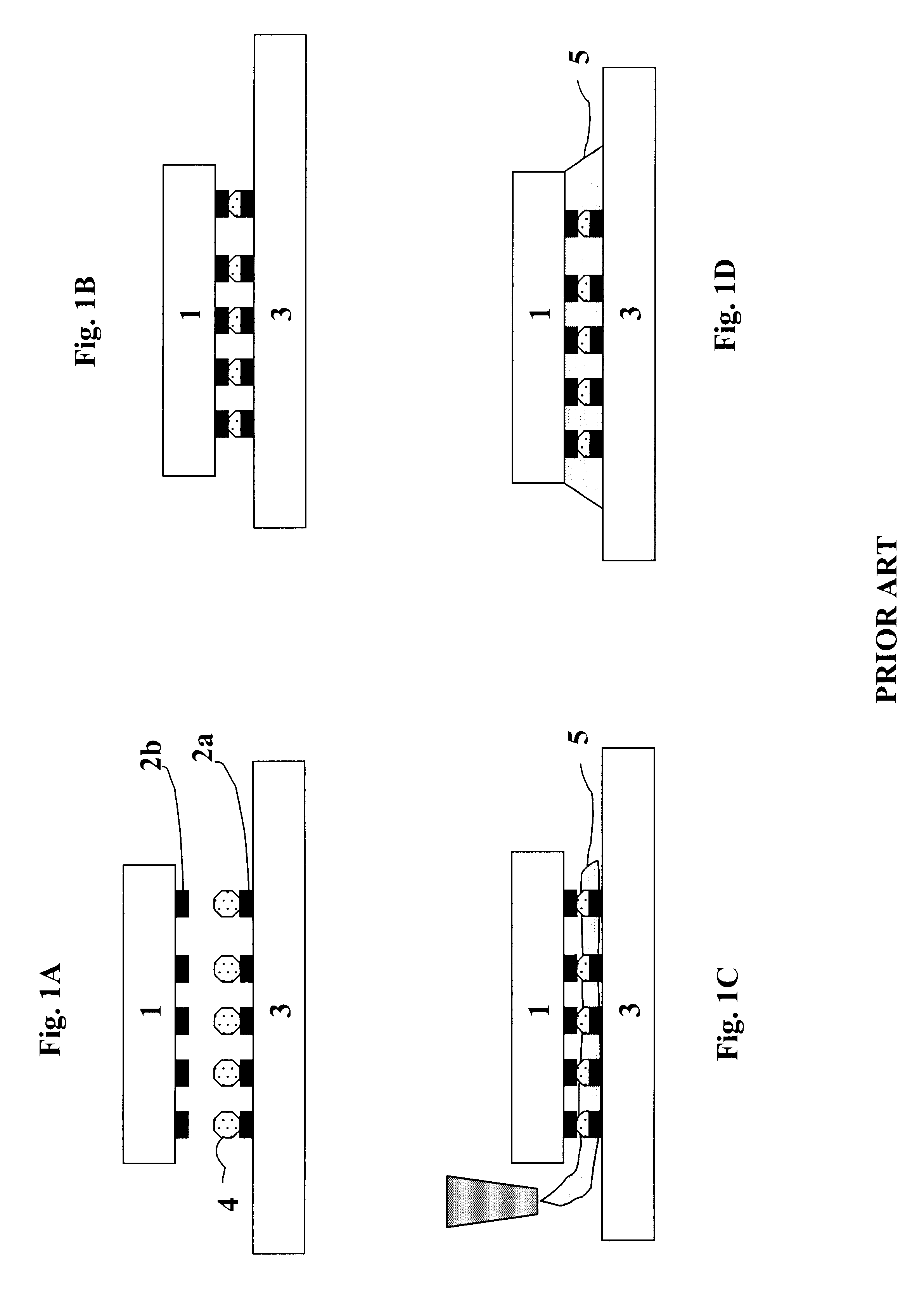
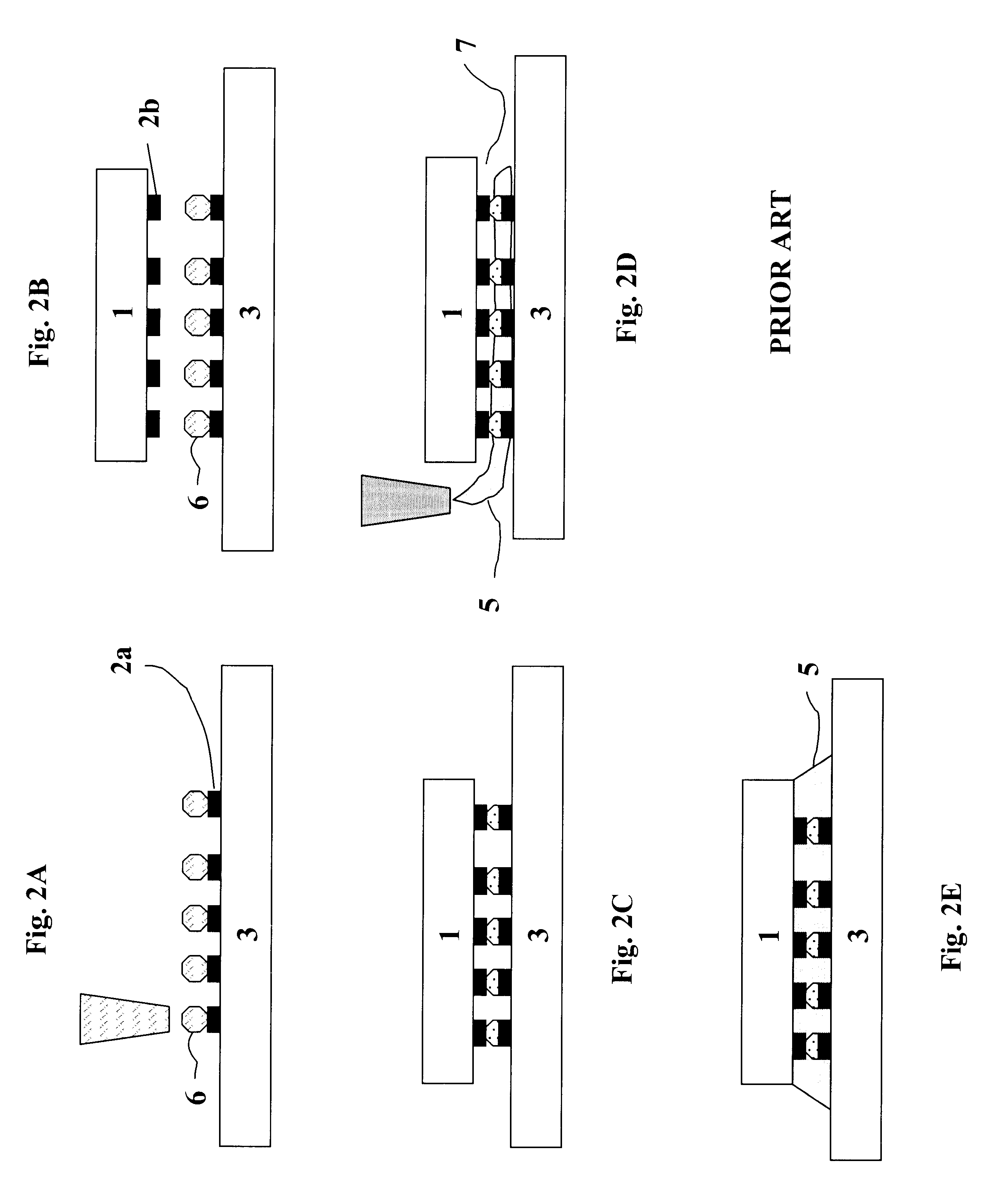
Step I1 (FIG. 4A): providing a substrate 3 comprising a plurality of metal areas called bonding or contact pads 2a and the chip 1, equally comprising a plurality of metal areas (2b) corresponding to said bonding pads (2a) on the substrate. The component's bonding pads (2b) can be chip bumps or pins.

Step I2 (FIG. 4B): Application of the ICA 6 on bonding pads 2a present on the substrate 3.

Step I3: Drying of the ICA.

Step I4 (FIG. 4C: cross section, FIG. 4D: top view): Application of NCA underfill material 5 to the substrate 3 in between the bonding pads 2a.

Step I5 (FIG. 4E): Alignment and placement of the component 1.

Step I6 (FIG. 4F): Execution of a thermocompression step to create electrical contacts between the component 1 and the substrate 3.

First the materials used in the above sequence are outlined; thereafter, the altern...

second embodiment

In the present invention, step I5, in which the component is positioned with respect to the substrate and placed on top of the adhesives, is done on a first tool. Again the component will be pushed to the adhesives present on the substrate, until the underfill material substantially fills in a uniform way the gap between both parts, not filled by the ICA bumps. The adherence of the component to the adhesives is such that the assembly can be transported to a second tool while maintaining the position of the component with respect to the substrate. Thanks to the presence of both the NCA and ICA adhesives, possible mechanical stress will be absorbed by both adhesives. The last step, step I6, in which the final electrical and mechanical connections are established is executed on a second tool according to the previous embodiment of the invention. By allowing the placement of the chip and the thermocompression cycle to be executed on two different machines, the throughput of an assembly ...

third embodiment

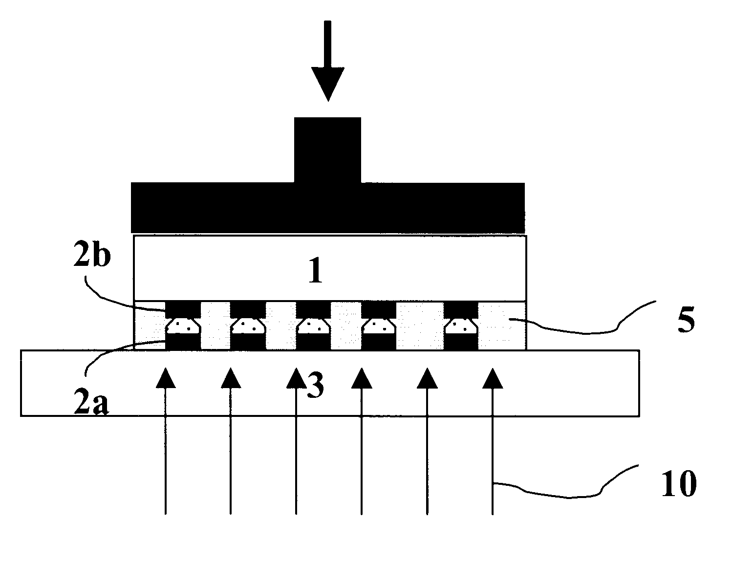
In the present invention, the curing of the adhesives, thereby establishing an electrical and mechanical connection, is done by ultraviolet (UV) light. This is illustrated in FIGS. 5A-5C. Instead of providing the energy necessary to form the cross links during the polymerisation of the adhesives by the thermode in contact with the component or to the substrate in contact with the supporting table, this energy can be provided for by light, preferably UV-light 10. If a transparent substrate 3, such as e.g. glass or plastic is used, which allows the passage of, e.g. UV radiation without absorbing the light, light curing can be used instead of thermal curing. A first requirement is that the adhesives must be UV curable. If the component is not transparent to the UV radiation, the curing can be executed from the backside of the assembly, i.e. the surface of the substrate opposite the surface connected to the component by applying heat to this surface. For example the table on which the s...


PUM


Abstract

The present invention is related to a flip-chip-on-board (FCOB) assembly technology applicable for mounting large chips with high I/O count or small pitch, mounted on low-cost or low-grade substrates. The assembly technology uses both an isotropically conductive adhesive (ICA) and a non-conductive material (NCA) in the same assembly cycle. The thermocompression step establishes at the same time the electrical and mechanical interconnections and the curing of the adhesives.

Description

The present invention relates to a method for assembling semiconductor devices on a substrate, such as a PCB substrate (printed circuit board), using a flip-chip assembly technique.Printed-circuit-board (PCB) assemblies, such as for telecommunications applications, are designed and produced with a high reliability as an important criterion. Therefore the technologies, applied in these assemblies, are often limited to well established and qualified technologies like reflow and wave soldering of standard SMT (surface-mount-technologies) and through-hole components. However, increasing demands for miniaturization, higher functionality, higher number of pins and higher frequencies put pressure on the telecommunications equipment manufacturers to introduce more advanced packaging technologies such as BGA (ball-grid-array), CSP (chip-size-package) and flip-chip assembly. These assembly techniques must cope with the requirements of, for example, larger chip size, increased number of pins o...

Claims


Application Information

Patent Timeline
Patent Type & Authority Patents(United States)
IPC IPC(8): H01L21/60H01L21/56H01L21/02H01R43/20H05K3/32H05K3/34
CPCH01L21/563H01L24/83H01L24/29H01L24/81H01L2924/07802H01L2224/16225H01L2224/73203H01L2224/73204H01L2224/81801H01L2224/83102H01L2224/83192H01L2224/838H01L2224/92125H01L2924/01004H01L2924/01005H01L2924/01013H01L2924/01029H01L2924/01033H01L2924/01047H01L2924/0105H01L2924/01078H01L2924/01079H01L2924/01082H01L2924/01322H01L2924/01327H01L2924/0781H01L2924/09701H01L2924/10329H01L2924/19041H01L2924/19043H01L2224/2919H01L2924/01006H01L2924/01076H01L2924/014H01L2924/0665H01L2924/07811H01L2224/32225H01L2924/0132H01L2924/1579H01L2224/29111H01L2924/10253H01L2924/00H01L2924/00012H01L2924/351H01L2224/05573H01L2224/05568H01L2224/05139H01L2224/05144H01L2224/05647H01L2224/05669H01L24/05H01L2924/00014
Inventor VANFLETEREN, JANSTOUKACH, SERGEIVANDECASTEELE, BJORN
Owner INTERUNIVERSITAIR MICRO ELECTRONICS CENT (IMEC VZW)
Why Eureka
Try Eureka