Thin-film solar array system and method for producing the same

a solar array and thin film technology, applied in photovoltaic energy generation, diodes, electrical equipment, etc., can solve the problems of only being able to realize this single-side grid, not conductive, and limited ewt cell to solar cells made of silicon disks

Inactive Publication Date: 2003-05-06
FRAUNHOFER GESELLSCHAFT ZUR FOERDERUNG DER ANGEWANDTEN FORSCHUNG EV
View PDF2 Cites 108 Cited by
  • Summary
  • Abstract
  • Description
  • Claims
  • Application Information

AI Technical Summary

Problems solved by technology

However, many such substrates 2 are not conductive.
Hitherto realization of this single-side grid has only been possible by means of very complicated processes.
Placing the respective metal contacts precisely on the corresponding zones poses a critical alignment problem and also requires masks, which must be accurately aligned.
However, an EWT cell is limited to solar cells made of silicon disks respectively wafers.
As a carrier substrate is a prerequisite for these thin-layer solar cells, their back surface is not accessible and the known EWT process cannot be applied.
At the same time, due to this minimal thickness, thin-layer cells permit using silicon of poorer quality than for conventional or EWT solar cells.
This is not possible, for example, with the previously mentioned EWT solar cells.

Method used


Image

  • Thin-film solar array system and method for producing the same
  • Thin-film solar array system and method for producing the same
  • Thin-film solar array system and method for producing the same

Examples


Embodiment Construction

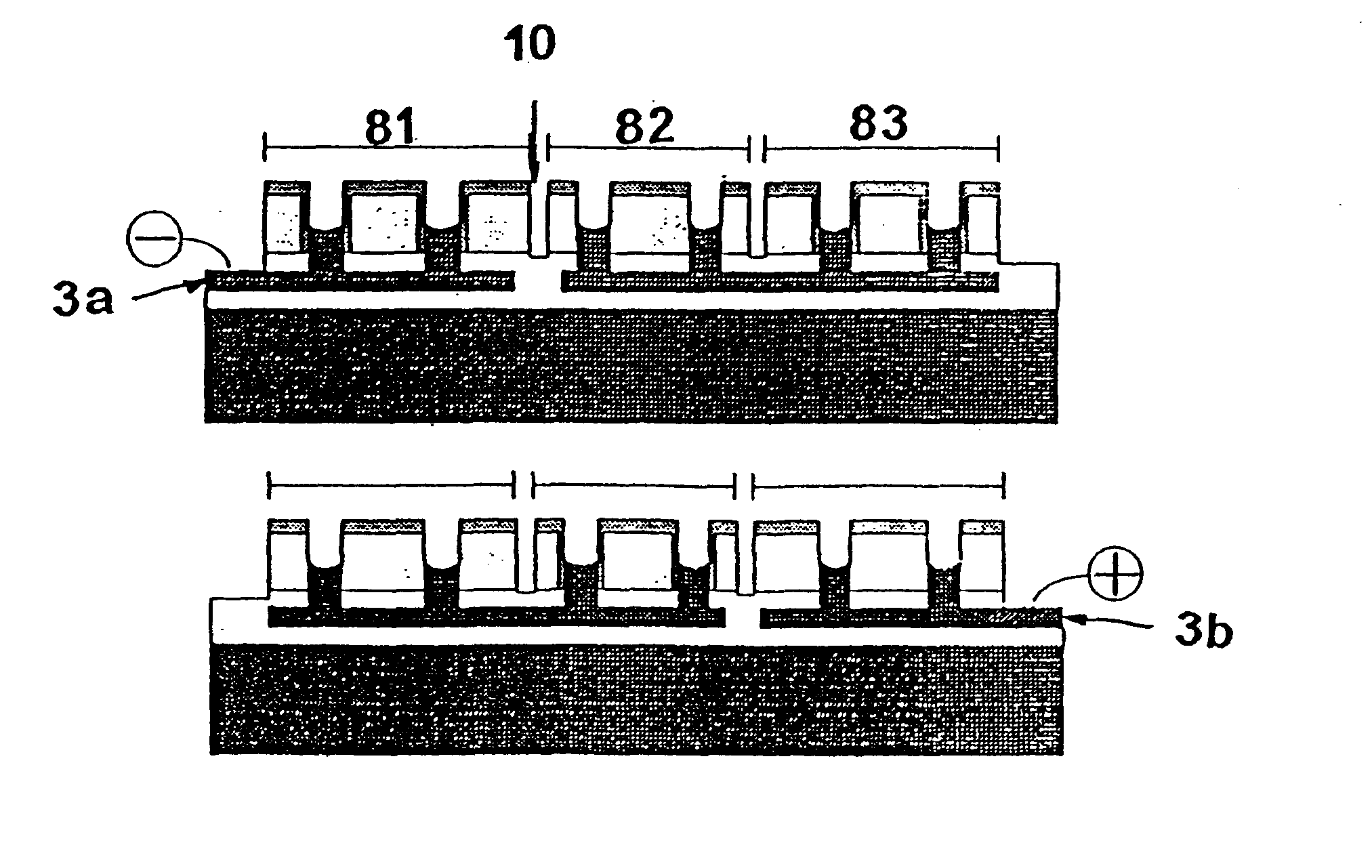
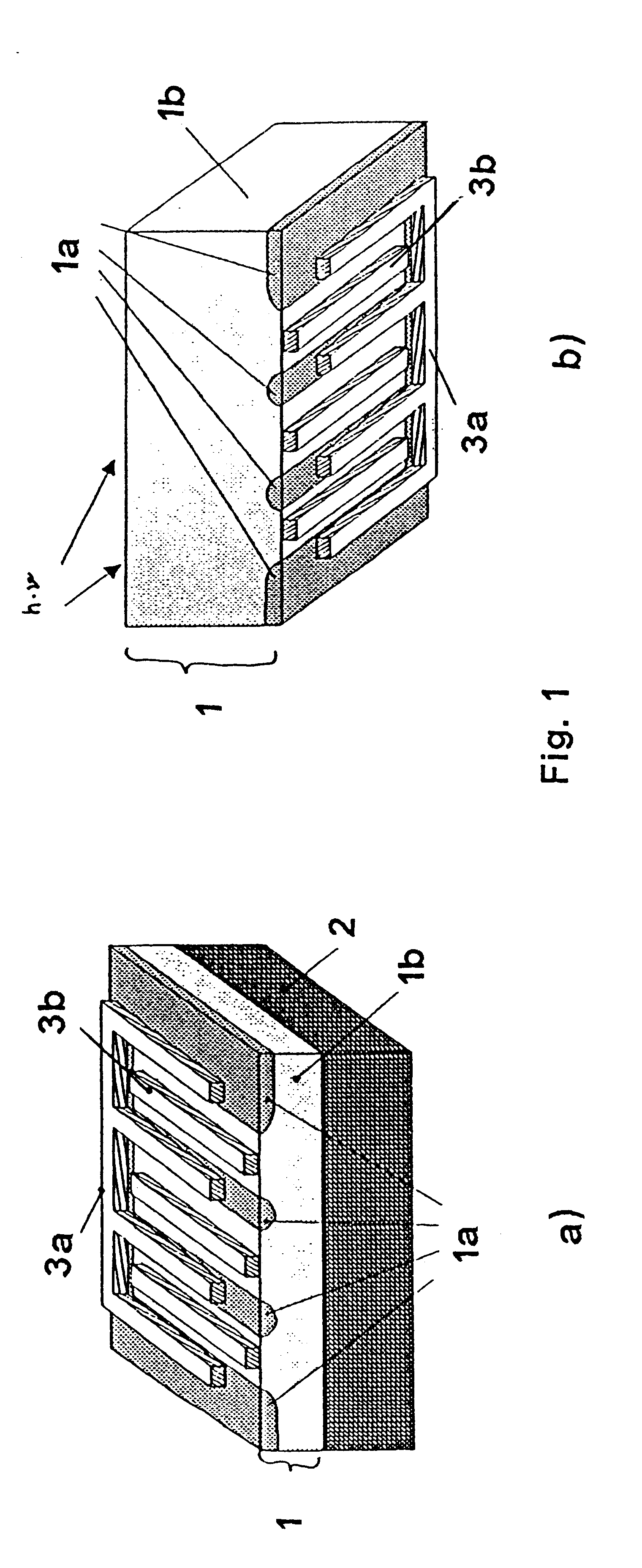
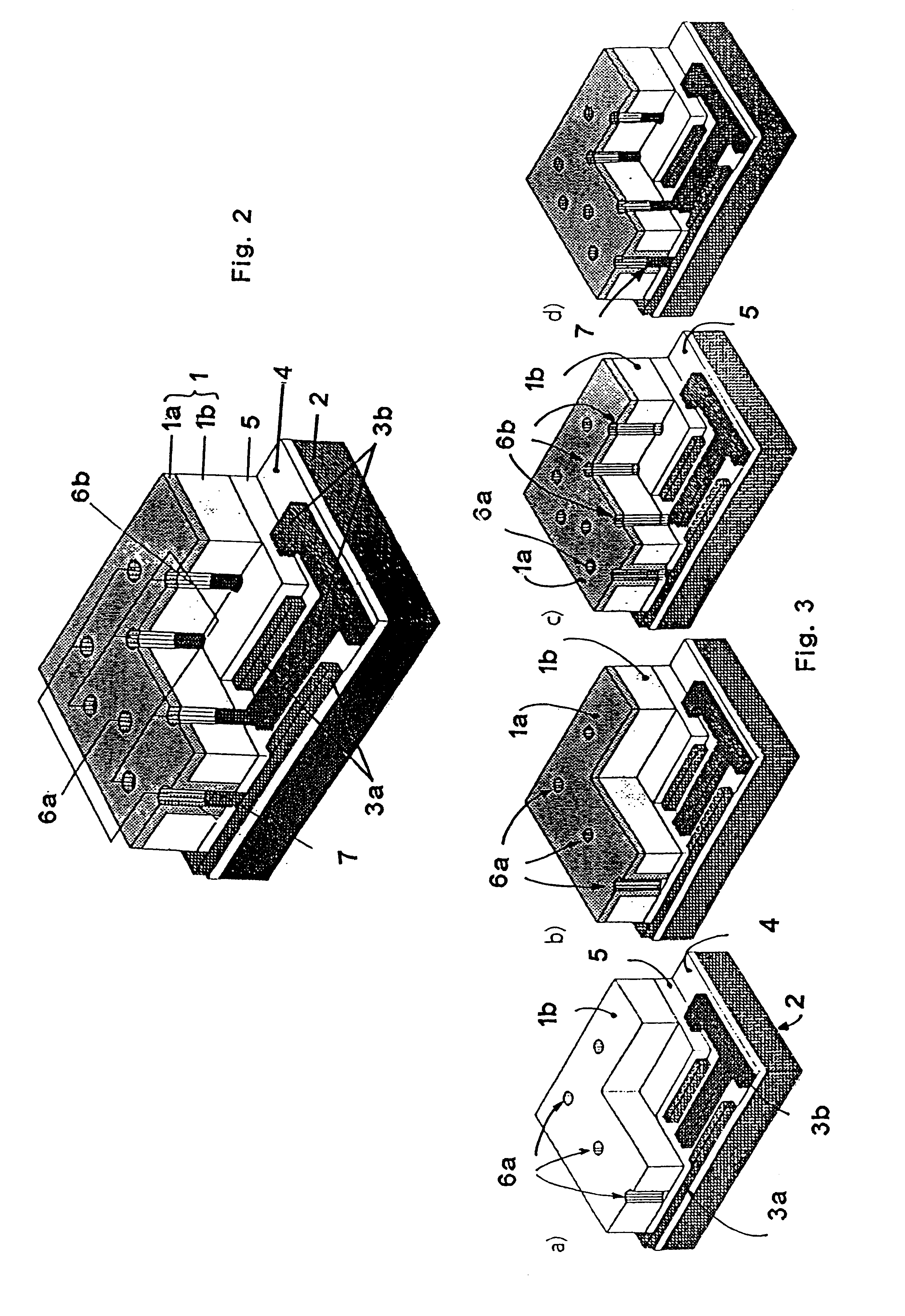
FIG. 2 shows the principle setup of the invented back-contact thin-layer solar cell (BC-TFC, Engl. Back-contact thin-layer) of the present invention.

Before deposition of the active solar cell layer 1, strip conductors 3a and 3b made of metal or other conductive materials, such as e.g. silicides (e.g. TiSi.sub.2) are directly applied to a carrier substrate 2 or to lower insulation layer 4. These strip conductors are covered with an upper electrical insulation layer 5 (for example, made of nitrides and / or oxides and / or carbides). In addition to electric insulation, the purpose of this layer 5 is to encapsulate the metal of the contact electrodes 3a and 3b, because it can melt in the subsequent temperature steps (e.g. during deposition of the active semiconductor layer or during formation of an emitter). Encapsulation ensures that the metal neither runs nor that large amounts of the metal diffuse through the insulation layer and adversely effect the quality of the active layer in this ...


PUM


Abstract

Disclosed is a thin-layer solar cell array system and a method for producing the same, having placed over a carrier substrate of plane design, a solar cell layer which is provided with at least one n-type conducting semiconductor zone (emitter) and at least one p-type conducting semiconductor zone (base) as well as a first and a second contact electrode, each of different electric polarity, which are each electrically connected to the emitter respectively to the base.The invention is distinguished by at least the first contact electrode being applied directly on the carrier substrate or separated by an electrically insulating layer, an electrically insulating layer being provided thereupon, and the solar cell layer being placed over the insulating layer, by at least one contact channel extending through the insulating layer and/or the solar cell layer in such a manner that the first contact electrode and the semiconductor layer zone of respective polarity inside the solar cell layer being electrically connectable by means of an electrically conducting material provided inside the contact channel, and by the second contact electrode like the first contact electrode being placed above or in the case of a conductive carrier layer also under the carrier layer and under the electrically insulating layer and the solar cell layer, and by at least one contact channel extending through the insulating layer and/or the solar cell layer in such a manner that the second contact electrode and the semiconductor layer zone of respective polarity inside the solar cell layer being electrically connected by means of an electrically conducting material provided inside the contact channel.

Description

1. Field of the InventionThe present invention relates to a thin-film solar cell array system and a method for producing the same.2. Description of the Prior ArtSolar cells are components which convert light into electric energy. Usually they comprise a semiconductor material containing n-type and p-type zones, i.e. zones in which current is transported by means of respectively negative and positive charge carriers. These zones are referred to respectively as the emitter and the base. The positive and negative charge carriers generated by incident light are separated and can be conveyed by means of metallic contacts on the respective zones. Only those charge carriers contribute to useable electric power that reach the contacts and do not recombine with a charge carrier of reverse polarity. A further loss mechanism is the reflection of light at the metal contacts, referred to as contact shading the solar cell. The smaller the shading, i.e. the more light which is able to reach the so...

Claims


Application Information

Patent Timeline
Patent Type & Authority Patents(United States)
IPC IPC(8): H01L29/02H01L29/22H01L31/06H01L31/0224H01L31/0392H01L31/068H01L31/036H01L31/04H01L31/18H01L27/142H01L31/05
CPCH01L27/142H01L31/022425H01L33/382H01L31/0682H01L31/022458H01L31/0516Y02E10/547
Inventor LUDEMANN, RALF
Owner FRAUNHOFER GESELLSCHAFT ZUR FOERDERUNG DER ANGEWANDTEN FORSCHUNG EV
Why Eureka
Try Eureka