Semiconductor package having heat sink at the outer surface

a technology of semiconductor devices and heat sinks, which is applied in the direction of semiconductor devices, semiconductor/solid-state device details, electrical apparatus, etc., and can solve problems such as affecting the performance of electronic devices

Inactive Publication Date: 2003-05-06
SILICONWARE PRECISION IND CO LTD
View PDF12 Cites 294 Cited by
  • Summary
  • Abstract
  • Description
  • Claims
  • Application Information

AI Technical Summary

Benefits of technology

It is another objective of the present invention to provide a semiconductor package that can easily add an external heat dissipator in order to improve the heat-dissipating efficiency of the package further.
It is one other objective of the present invention to provide a semiconductor package having stacked chips in order to improve the heat-dissipating efficiency of the package and to enhance the performance of the electronic devices.
According to a preferred embodiment of the present invention, a heat sink and an external heat dissipator can be added to further improve the package's heat-dissipating efficiency. The heat sink is bonded to the back surface of the chip while exposed on the bottom surface of the package structure. And the external heat dissipator is mounted on the exposed surface of the die pad.
According to another preferred embodiment of the present invention, a heat sink and an external heat dissipator can be added to the stacked chip package to further improve the package's heat-dissipating efficiency. The heat sink is bonded to the active surface of the second chip while exposed on the bottom surface of the package structure. And the external heat dissipator is mounted on the exposed second surface of the die pad.

Problems solved by technology

Therefore, just how to provide the semiconductor package with even more effective heat-dissipating path has become an important issue in order to improve the performance of the semiconductor devices.
Therefore, the conventional package structure is unable to dissipate the heat effectively, as a result, the performance of the electronic devices will be affected.

Method used


Image

  • Semiconductor package having heat sink at the outer surface
  • Semiconductor package having heat sink at the outer surface
  • Semiconductor package having heat sink at the outer surface

Examples


Embodiment Construction

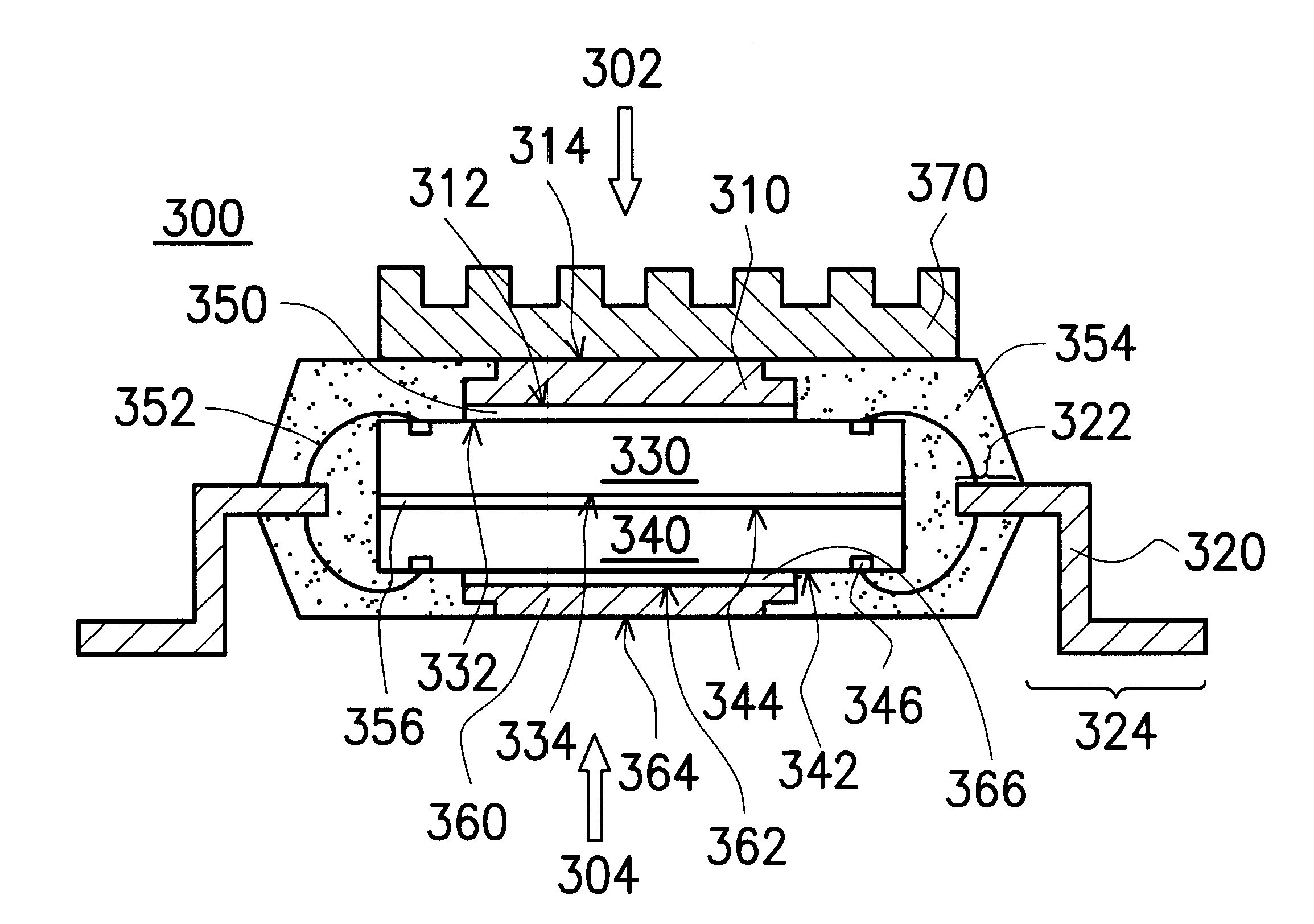
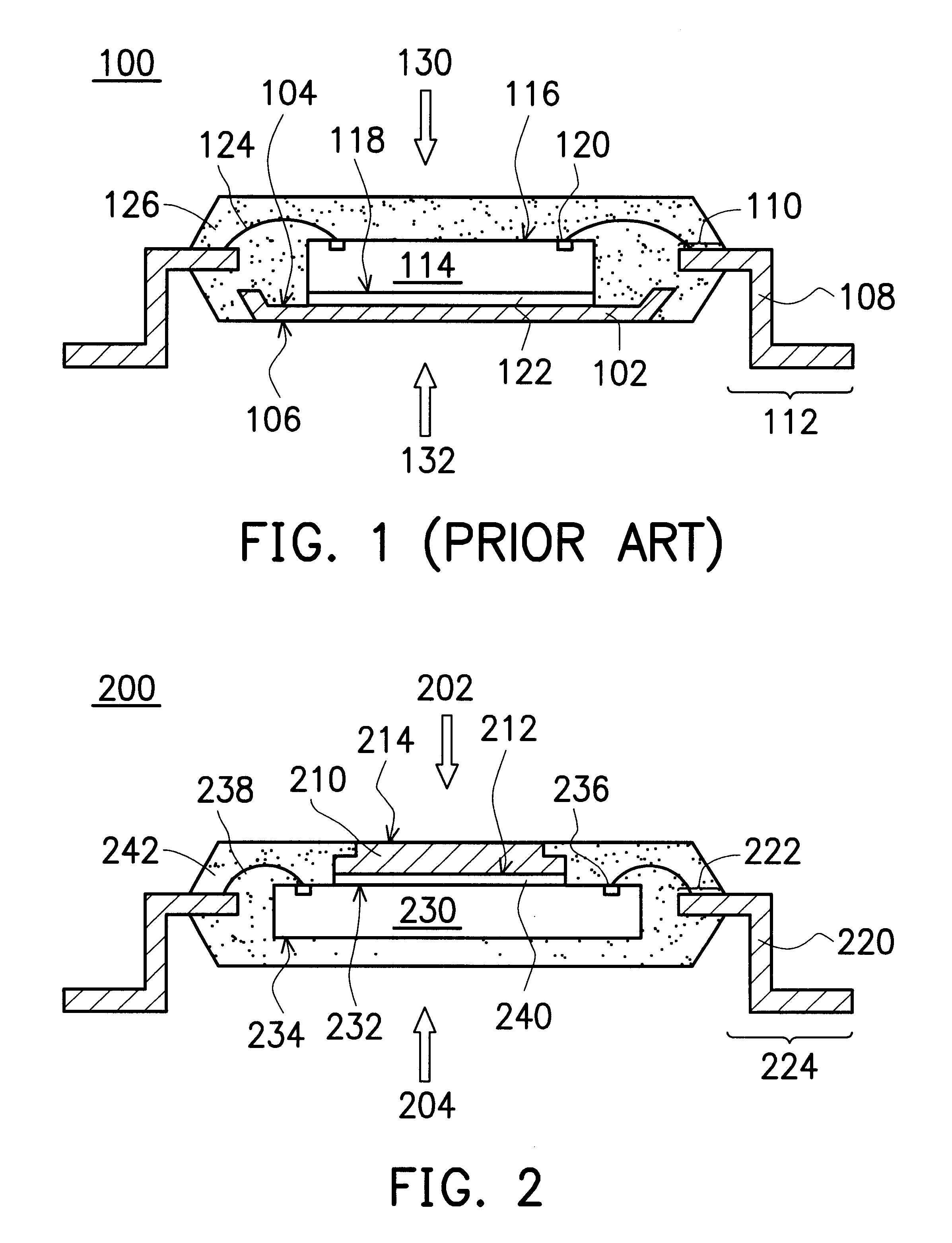
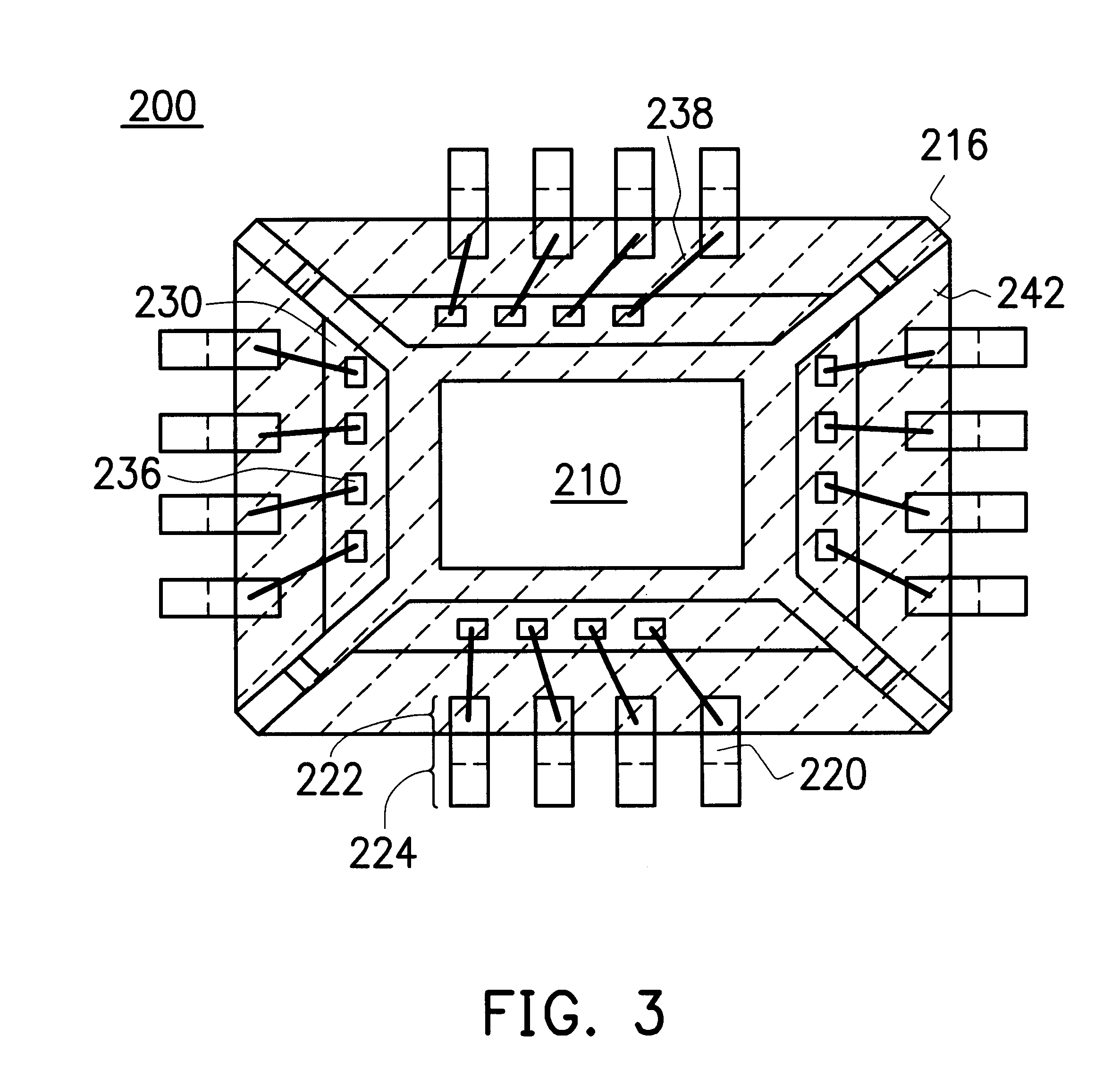
FIG. 2 is a schematic cross-sectional view of a semiconductor package having a heat sink at the outer surface of the first preferred embodiment according to the present invention while FIG. 3 is a top view of FIG. 2 according to the present invention. As shown in FIG. 2, and FIG. 3, a semiconductor package of the first preferred embodiment according to the present invention is constructed on a lead frame that is constituted by a die pad 210 and a plurality of leads 220 disposed on the periphery of the lead frame. The die pad 210 has a first surface 212 (bottom surface) and a second surface 214 (top surface) while the lead 220 has an inner lead portion 222 and an outer lead portion 224. There are tie bars 216 disposed on the periphery of the die pad 210 for connecting the die pad 210 to the guide rail (not shown) of the lead frame. And through the upset of the tie bars 216, the die pad 210 and the leads 220 are on different planes. The die pad 210 is preferably formed a stepped struc...


PUM


Abstract

A semiconductor package having heat sink at the outer surface is constructed on a lead frame. The package comprises a chip, a die pad, a plurality of leads, a plurality of bonding wires, and a molding compound. The die pad has a first surface and a second surface, and the chip has its active surface bonded to the first surface of the die pad. The area of the die pad is smaller than the area of the chip in order to expose the bonding pads on the active surface of the chip. The leads having an inner lead portions and an outer lead portions are disposed at the periphery of the die pad, and the inner lead portions are electrically connected to the bonding pads by a plurality of bonding wires. The molding compound encapsulates the chip, the die pad, the inner lead portions of the leads, and the bonding wires. The second surface of the die pad is exposed on the top surface of the package structure while the outer lead portion of the leads is exposed at the side edge of the package structure.

Description

1. Field of the InventionThis invention relates to a semiconductor package having heat sink at the outer surface, and more particularly to a semiconductor package having heat sink at the outer surface that can enhance the heat-dissipating effect.2. Description of Related ArtFollowing the evolution of the integrated circuit technology, the manufacturing process of integrated circuit has been advanced to ever high in integration with a target of pursuing ever dense on the design of the package structure for the packaging process in the back end process. Owing to the demand of high speed on the data processing, the signal frequency of semiconductor devices is getting higher and higher. Together with the increase in the integration of semiconductor and the package density, the heat generation per unit time per unit volume has increased significantly. Therefore, just how to provide the semiconductor package with even more effective heat-dissipating path has become an important issue in o...

Claims


Application Information

Patent Timeline
Patent Type & Authority Patents(United States)
IPC IPC(8): H01L23/48H01L23/34H01L23/433H01L23/495
CPCH01L23/4334H01L23/49575H01L2224/32257H01L2224/48091H01L2224/48247H01L2224/49171H01L2924/01079H01L2924/14H01L2924/3011H01L2224/45124H01L2224/32245H01L2224/73215H01L24/48H01L24/49H01L2224/73265H01L2224/45144H01L2924/00014H01L2924/00H01L24/45H01L2224/05553H01L2224/32145H01L2224/4826H01L2924/181H01L2224/05599H01L2924/00012
Inventor HUANG, CHIEN-PING
Owner SILICONWARE PRECISION IND CO LTD
Why Eureka
Try Eureka