Insulation barrier on a printed circuit board
- Summary
- Abstract
- Description
- Claims
- Application Information
AI Technical Summary
Benefits of technology
Problems solved by technology
Method used
Image
Examples
Embodiment Construction
Throughout the drawings, the same reference characters will be used for corresponding or similar elements.
It should be understood that the term "printed circuit board" should not be interpreted in a limited sense as restricted to a circuit board with "printed" components, but rather in a broad sense as any type of conventional circuit board.
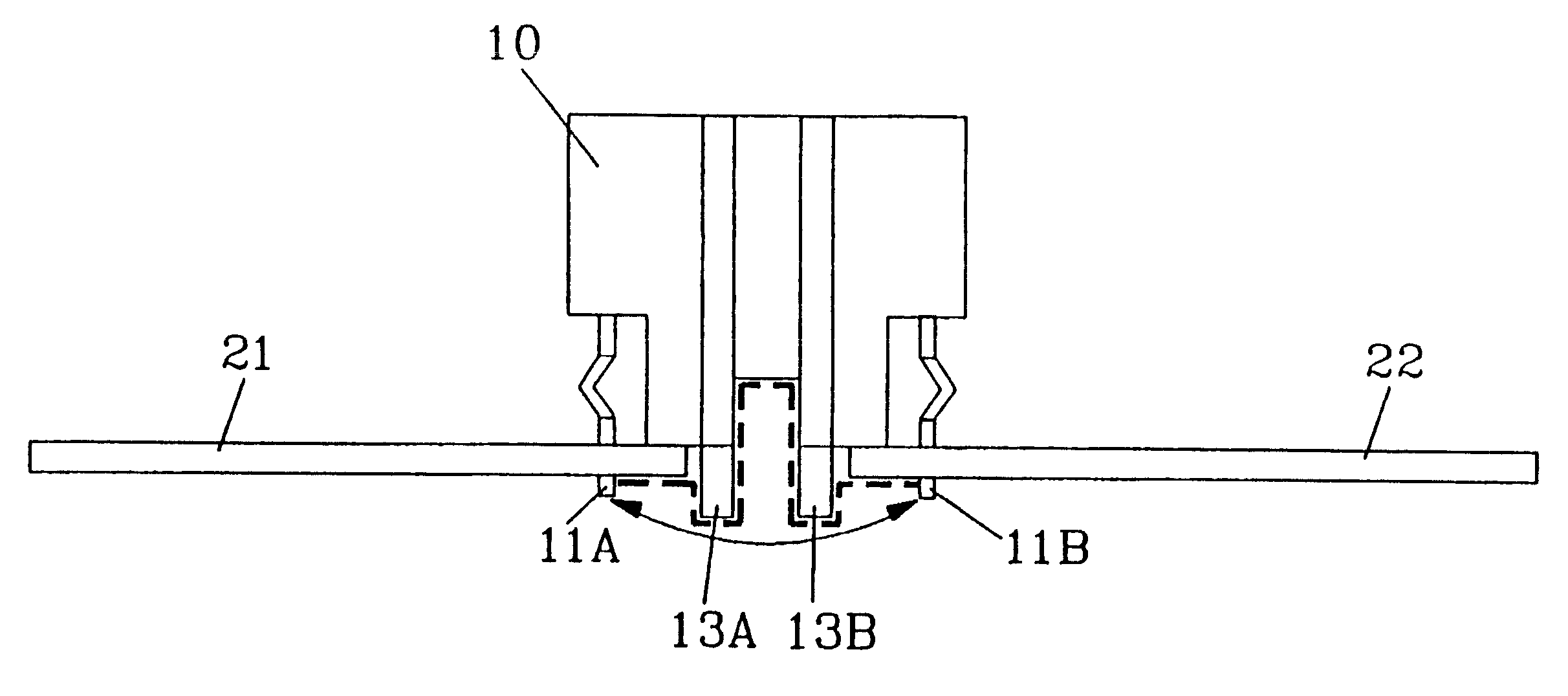
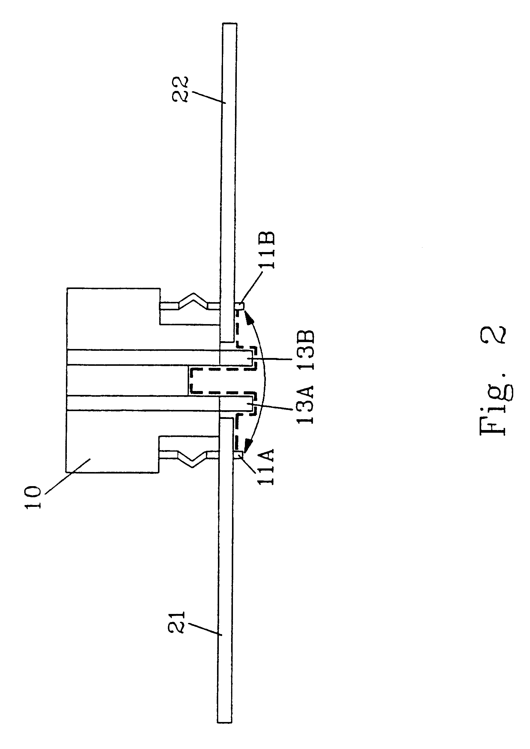
FIG. 2 is a schematic diagram of a printed circuit board assembly according to a first preferred embodiment of the invention. As can be seen in FIG. 2, the printed circuit board is divided into two separate sections 21, 22, which are interconnected by an insulation transformer 10. In general, each PCB section carries a number of electrical components that constitute a respective electrical system. The transformer 10 has a number of transformer pins 11A on the primary side of the transformer, and a number of transformer pins 11B on the secondary side of the transformer. Preferably, the pins 11A, 11B are through-hole soldered to the PCB sections 21...
PUM
| Property | Measurement | Unit |
|---|---|---|
| Size | aaaaa | aaaaa |
| Distance | aaaaa | aaaaa |
Abstract
Description
Claims
Application Information


