Memory elements and methods for making same

a technology applied in the field of memory elements and methods for making same, can solve the problems of memory cells with different operational characteristics, insufficient known fabrication techniques, and inability to achieve high-density memory products

Inactive Publication Date: 2003-05-13
ROUND ROCK RES LLC
View PDF80 Cites 402 Cited by
  • Summary
  • Abstract
  • Description
  • Claims
  • Application Information

AI Technical Summary

Problems solved by technology

However, known fabrication techniques have not proven sufficient.
Unfortunately, electrically popping the thin silicon nitride layer is not desirable for a high density memory product due to the high current and the large amount of testing time required.
Furthermore, this technique may produce memory cells with differing operational characteristics, because the amount of dielectric breakdown may vary from cell to cell.

Method used


Image

  • Memory elements and methods for making same
  • Memory elements and methods for making same
  • Memory elements and methods for making same

Examples


Embodiment Construction

Specific embodiments of memory elements and methods of making such memory elements are described below as they might be implemented for use in semiconductor memory circuits. In the interest of clarity, not all features of an actual implementation are described in this specification. It should be appreciated that in the development of any such actual implementation (as in any semiconductor engineering project), numerous implementation-specific decisions must be made to achieve the developers' specific goals, such as compliance with system-related and business-related constraints, which may vary from one implementation to another. Moreover, it should be appreciated that such a development effort might be complex and time-consuming, but would nevertheless be a routine undertaking of semiconductor design and fabrication for those of ordinary skill having the benefit of this disclosure.

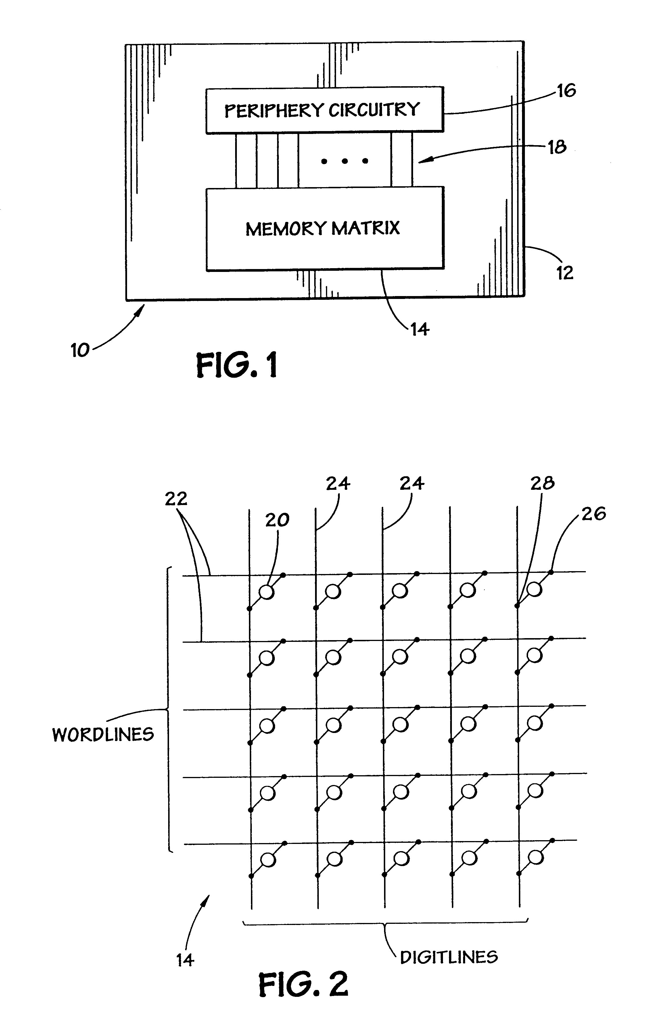
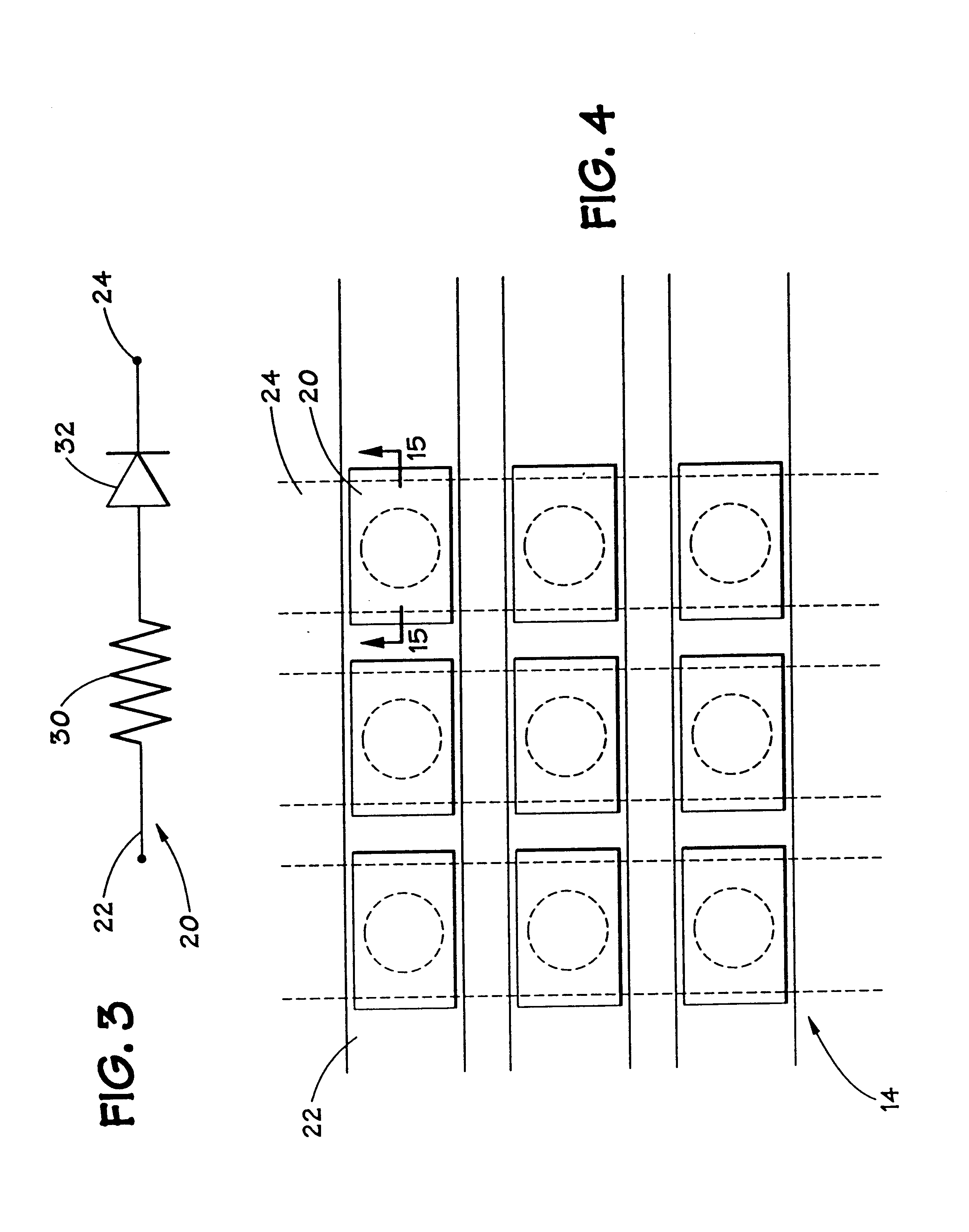
Turning now to the drawings, and referring initially to FIG. 1, a memory device is illustrated and gene...


PUM

PropertyMeasurementUnit
thickaaaaaaaaaa
programming voltageaaaaaaaaaa

Abstract

Annular, linear, and point contact structures are described which exhibit a greatly reduced susceptibility to process deviations caused by lithographic and deposition variations than does a conventional circular contact plug. In one embodiment, a standard conductive material such as carbon or titanium nitride is used to form the contact. In an alternative embodiment, a memory material itself is used to form the contact. These contact structures may be made by various processes, including chemical mechanical planarization and facet etching.

Description

1. Field of the InventionThe invention relates generally to the field of semiconductor devices and fabrication and, more particularly, to memory elements and methods for making memory elements.2. Background of the Related ArtThis section is intended to introduce the reader to various aspects of art that may be related to various aspects of the present invention, which are described and / or claimed below. This discussion is believed to be helpful in providing the reader with background information to facilitate a better understanding of the various aspects of the present invention. Accordingly, it should be understood that these statements are to be read in this light, and not as admissions of prior art.Microprocessor-controlled integrated circuits are used in a wide variety of applications. Such applications include personal computers, vehicle control systems, telephone networks, and a host of consumer products. As is well known, microprocessors are essentially generic devices that p...

Claims


Application Information

Patent Timeline
Patent Type & Authority Patents(United States)
IPC IPC(8): H01L45/00H01L27/24
CPCH01L29/45H01L45/06H01L45/1233H01L45/124H01L45/122H01L45/144H01L45/16H01L45/1691H01L27/2472H01L45/1273Y10S257/91H10B63/82H10N70/231H10N70/821H10N70/826H10N70/8265H10N70/8418H10N70/8828H10N70/011H10N70/068
Inventor HARSHFIELD, STEVEN T.
Owner ROUND ROCK RES LLC
Why Eureka
Try Eureka