Low voltage CMOS current source

A current source, low-voltage technology, applied in the field of low-voltage high-precision CMOS current source, can solve the problems of good combination, large process error of integrated reference resistance, inability to guarantee the reference current value and temperature coefficient, etc., to achieve small process deviation and good power supply. Effects of characteristics and temperature characteristics

Active Publication Date: 2009-10-21
陕西光电子先导院科技有限公司
View PDF0 Cites 20 Cited by
  • Summary
  • Abstract
  • Description
  • Claims
  • Application Information

AI Technical Summary

Problems solved by technology

[0003] At present, the commonly used current source design method is to generate a reference current based on the bandgap voltage reference source added to both ends of the reference resistor, but the process error of the integrated reference resistor is very large, such as the PCM parameter of the 0.6μm CMOS Poly2 resistor is 800±150 ohms per square , the reference current value and temperature coefficient cannot be guaranteed; and if an external reference resistor is used, it will not only increase the cost, but also cannot guarantee the consistency between the reference sources
The current technical solutions have not achieved a good combination of temperature characteristics and power characteristics, especially in the design of high-precision current sources with low power supply voltages is still blank, so it is necessary to adopt a new circuit structure to achieve high-precision current sources

Method used


Image

  • Low voltage CMOS current source
  • Low voltage CMOS current source
  • Low voltage CMOS current source

Examples


Embodiment Construction

[0034] First, in order to facilitate the understanding of the specific embodiments of the present invention, the following describes the technical terms involved in the specific embodiments of the present invention:

[0035] PMOS: P-channel Metal Oxide Semiconductor FET, P-channel Metal Oxide Semiconductor field effect transistor;

[0036] NMOS: N-channel Metal Oxide Semiconductor FET, N-channel metal oxide semiconductor field effect transistor.

[0037] Secondly, in order to make the objectives, technical solutions, and advantages of the embodiments of the present invention clearer, the following describes the embodiments of the present invention in further detail with reference to the embodiments and drawings. Here, the exemplary embodiments and description of the present invention are used to explain the present invention, but not as a limitation to the present invention.

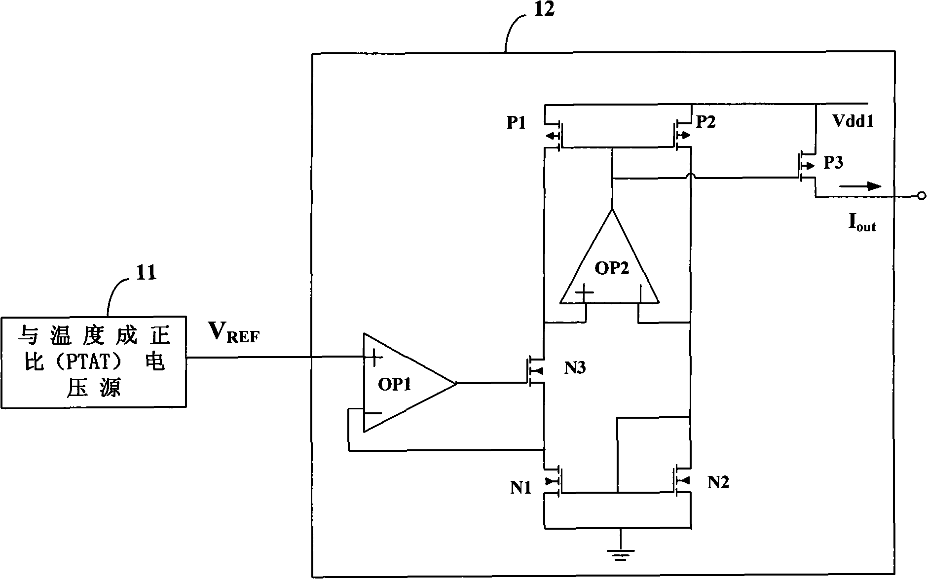
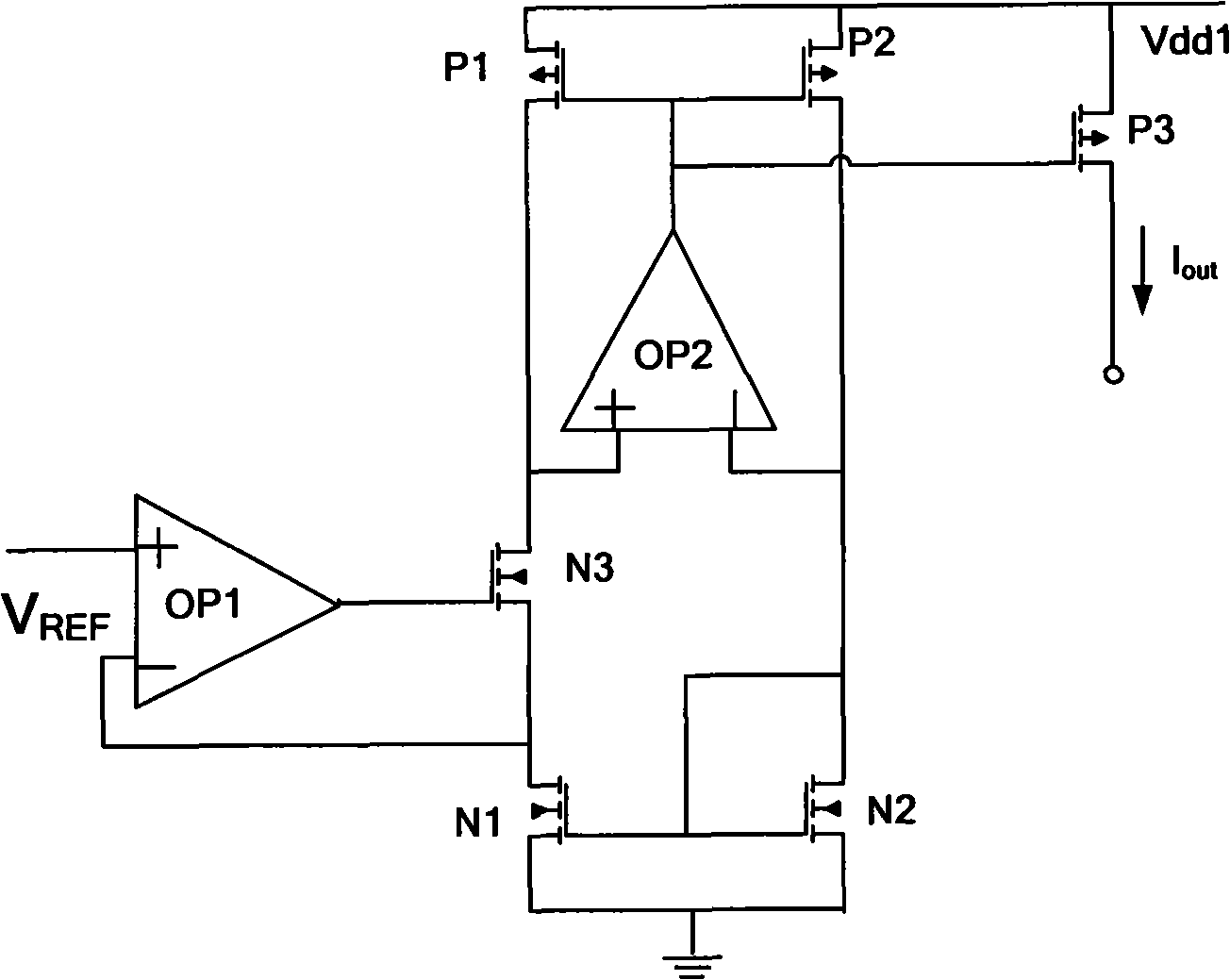
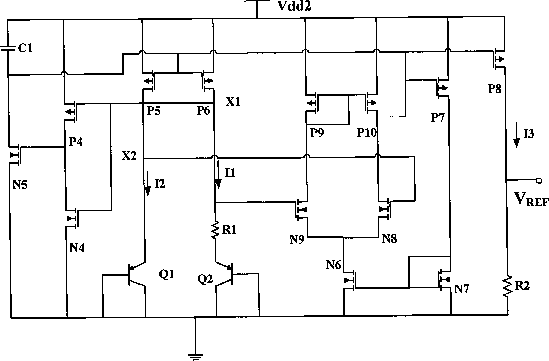
[0038] As shown figure 1 Shown is the circuit diagram of the low-voltage CMOS current source in this emb...


PUM


Abstract

The invention discloses a low voltage CMOS current source, and belongs to the field of analog integrated circuit. The low voltage CMOS current source comprises a PTAT voltage source, a current converting circuit and a mirror image circuit which are connected with the PTAT voltage source, wherein, the PTAT voltage source is used for generating a reference voltage V[REF] with a positive temperature coefficient; and the current converting circuit and the mirror image circuit are used for converting the reference voltage V[REF] into a reference current, and outputting the reference current by a current mirror relation. The low voltage CMOS current source has good power supply property and temperature property, and process deviation of the CMOS current source has little influence on an output current value of the CMOS current source.

Description

Technical field [0001] The invention relates to the field of analog integrated circuits, in particular to a low-voltage and high-precision CMOS current source. Background technique [0002] As a key circuit unit of analog integrated circuits, current sources are widely used in the design of mixed-signal integrated circuits such as A / D (analog / digital) converters, D / A converters and Viterbi decoders. [0003] At present, the commonly used current source design method is based on the bandgap voltage reference source to generate the reference current at both ends of the reference resistor, but the process error of the integrated reference resistor is very large, such as the 0.6μm CMOS Poly2 resistor PCM parameter is 800±150 ohms per square , The reference current value and temperature coefficient cannot be guaranteed; and if an external reference resistor is used, it will not only increase the cost, but also cannot guarantee the consistency between the reference sources. The current...

Claims


Application Information

Patent Timeline
Patent Type & Authority Applications(China)
IPC IPC(8): G05F3/26
Inventor 杨银堂朱樟明何芸李光辉刘帘曦
Owner 陕西光电子先导院科技有限公司
Why Eureka
Try Eureka