

Self aligning non contact shadow ring process kit
- Summary
- Abstract
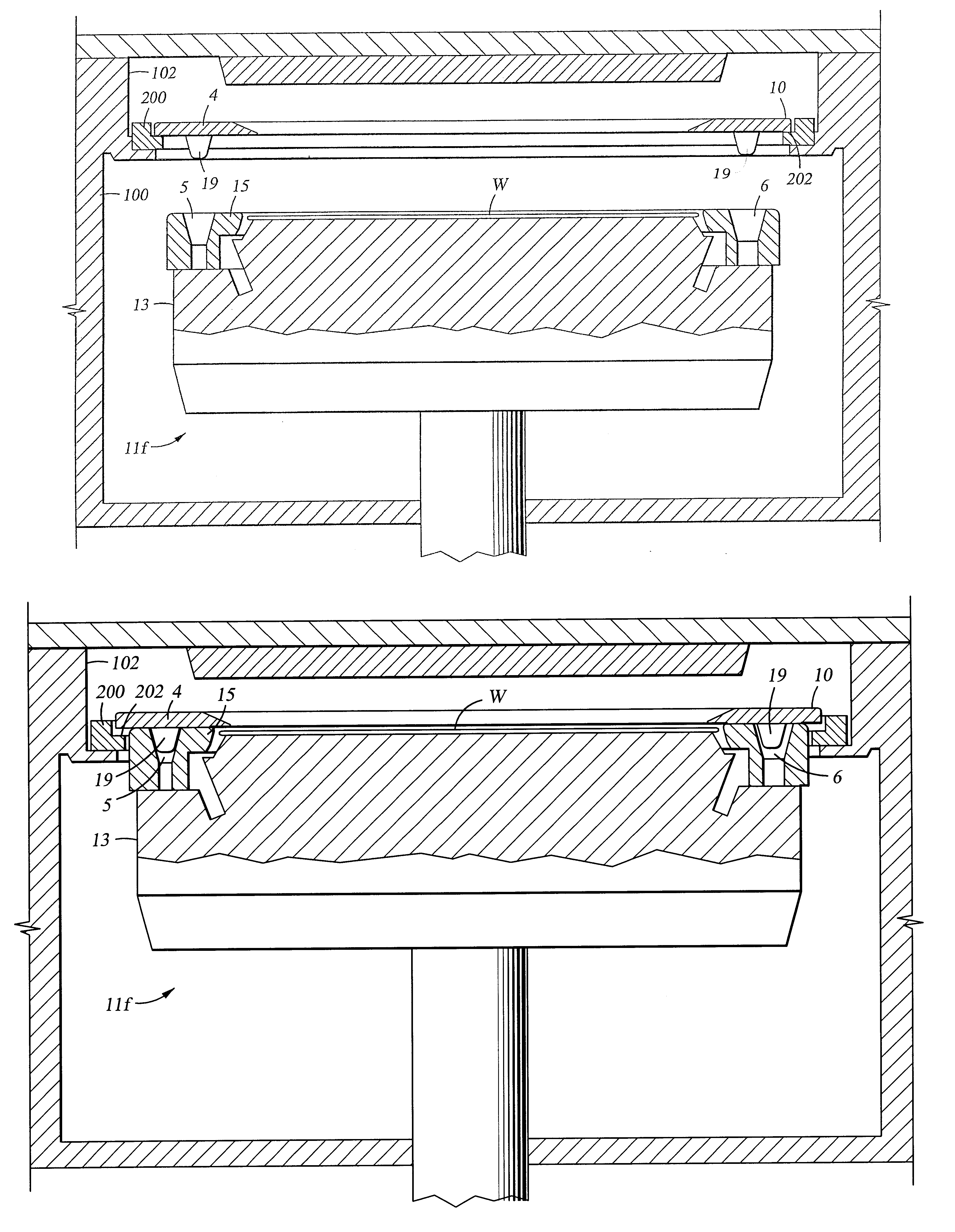
- Description
- Claims
- Application Information
AI Technical Summary
Problems solved by technology
Method used
Image

Examples
Embodiment Construction
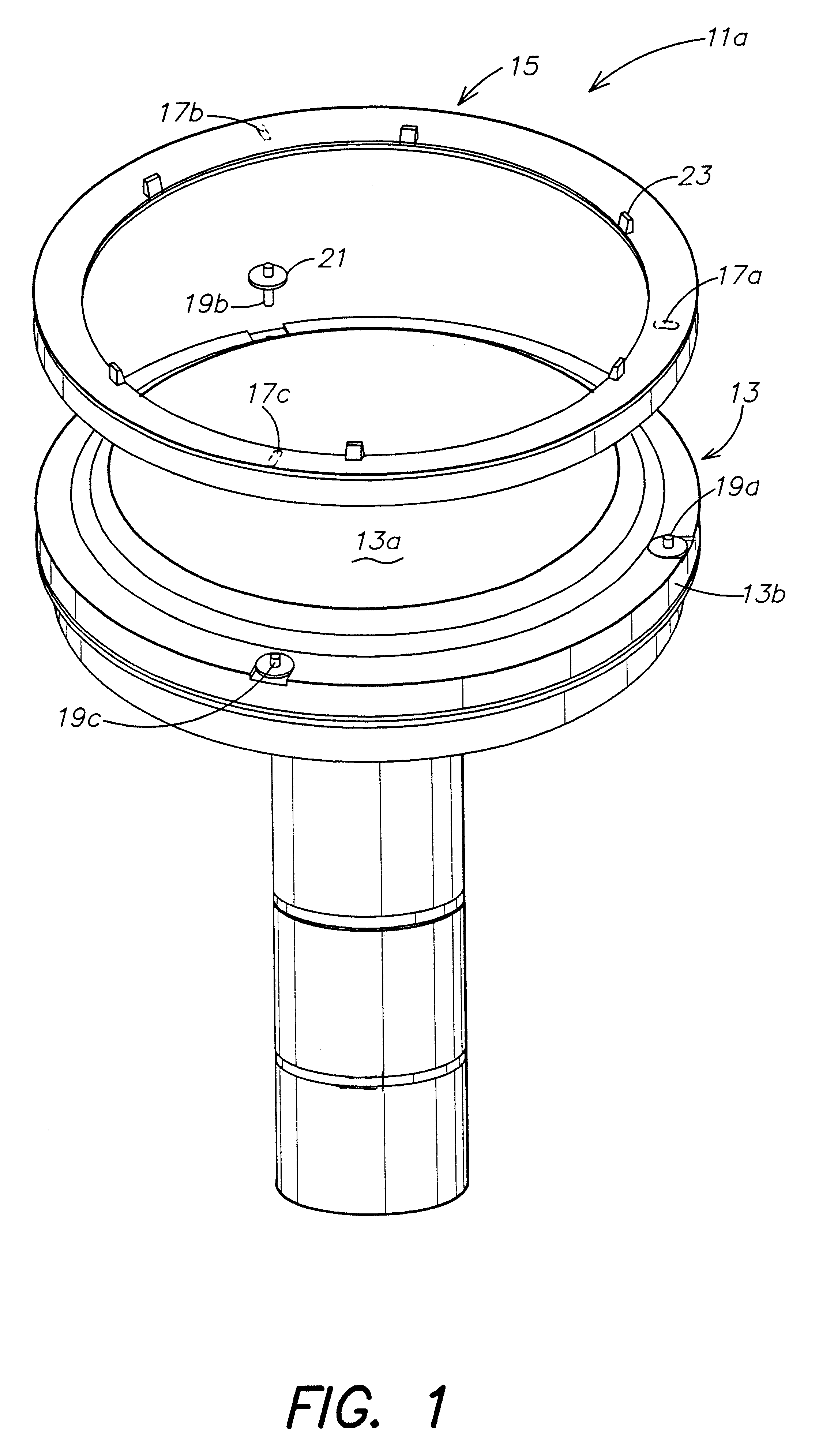
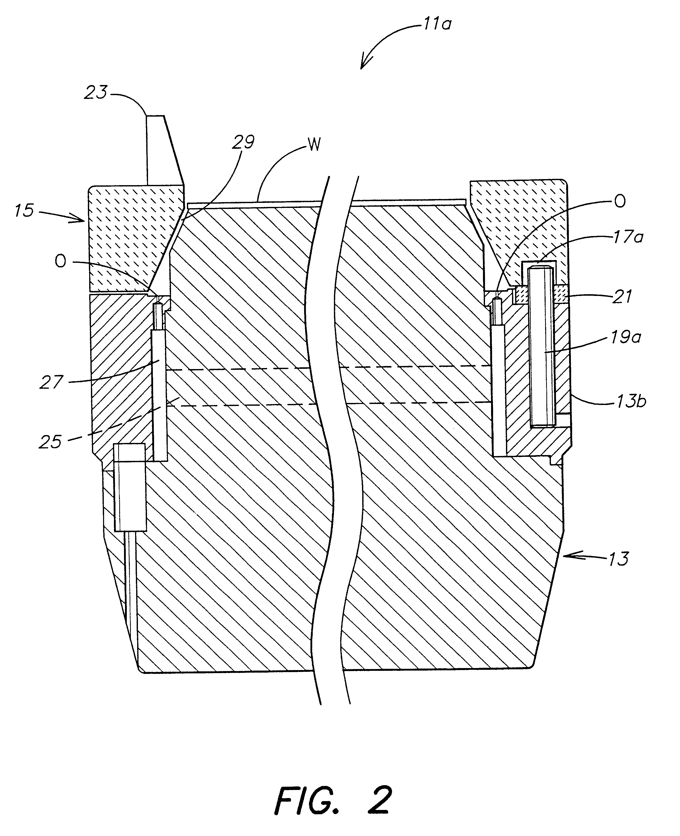
FIG. 1 is an exploded perspective view of a susceptor 11a. The susceptor 11a comprises a substrate support 13, adapted for pin and slot coupling with an edge ring, such as purge ring 15. Specifically, the substrate support 13 comprises three pins 19a-c which extend upwardly from the top surface of substrate support 13. The bottom surface of the purge ring 15 comprises three alignment slots 17a-c positioned to interface with the three pins 19a-c. The substrate support 13 comprises a central wafer supporting surface 13a, and the three pins 19a-c are disposed substantially equally spaced around the substrate supporting surface 13a. Each of the slots 17a-c is at least as wide as the corresponding pin 19a-c, and extends radially outward from the center of the substrate supporting surface 13a, in the direction in which the substrate support 13 expands and contracts during thermal cycling.
The substrate support 13 is preferably made of a metal such as aluminum, as is conventional. The purge...
PUM
| Property | Measurement | Unit |
|---|---|---|
| Length | aaaaa | aaaaa |
| Width | aaaaa | aaaaa |
| Width | aaaaa | aaaaa |
Abstract
Description
Claims
Application Information