Low-voltage differential driver with opened eye pattern

a low-voltage differential and eye pattern technology, applied in logic circuit coupling/interface arrangement, pulse technique, baseband system details, etc., can solve problems such as distortion, reducing the opening of eye pattern, and limiting performance of external signaling

Inactive Publication Date: 2003-07-08
DIODES INC
View PDF18 Cites 64 Cited by
  • Summary
  • Abstract
  • Description
  • Claims
  • Application Information

AI Technical Summary

Problems solved by technology

External signaling can often limit performance, such as when signals are driven from an integrated circuit (IC) to another IC.
Distortions can occur, further reducing the opening of the eye pattern due to jitter and noise of the cable environment.
This limits operation at higher frequencies.
This series resistance is undesirable as it can decrease the effectiveness of the boost current, adding delay and an I-R voltage drop.
Especially at higher frequencies this added series resistance can degrade performance.

Method used


Image

  • Low-voltage differential driver with opened eye pattern
  • Low-voltage differential driver with opened eye pattern
  • Low-voltage differential driver with opened eye pattern

Examples


Embodiment Construction

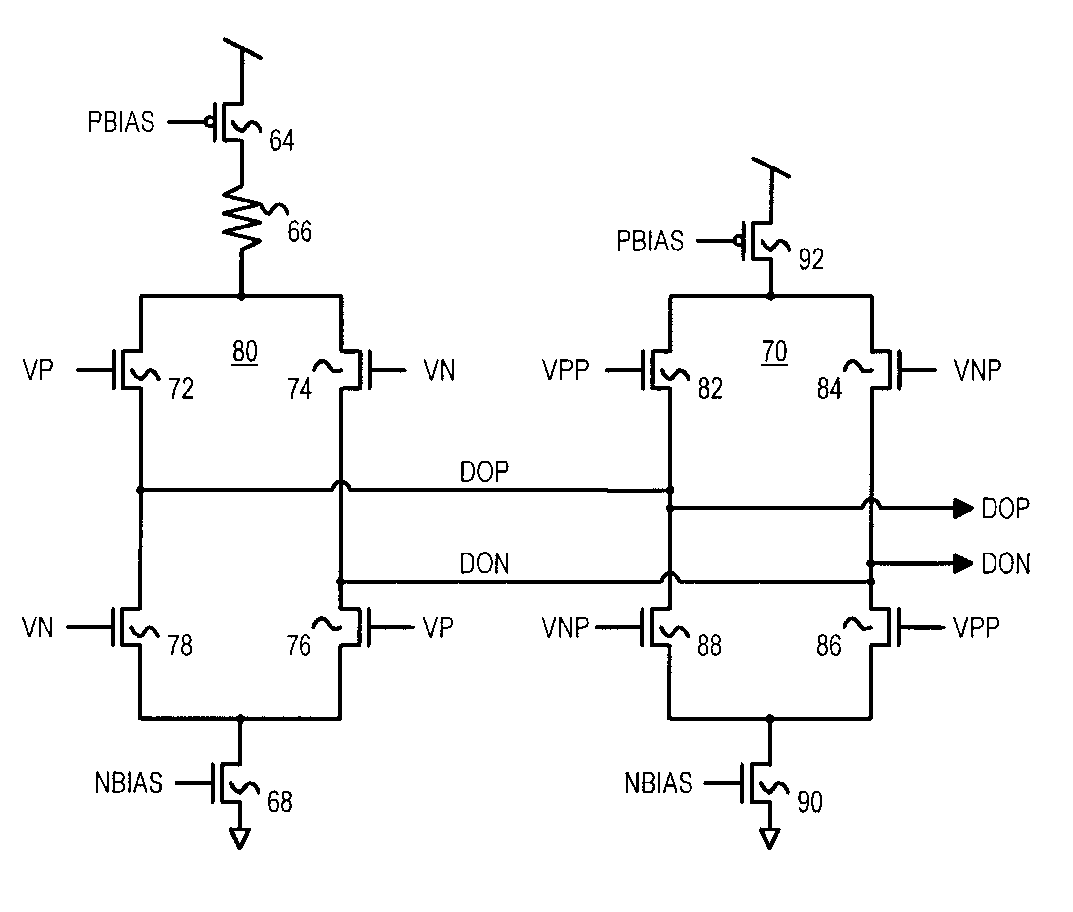
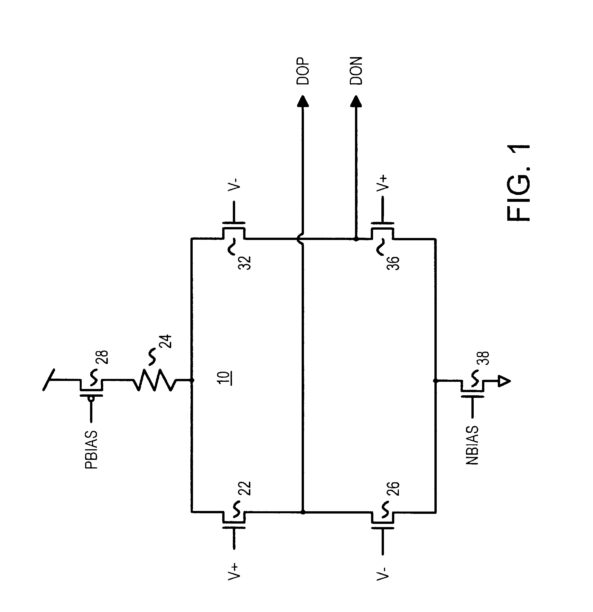
Several other embodiments are contemplated by the inventors. For example, different transistor sizes and biases can be used to obtain desired currents in the two stages. The load resistance may be chosen by the system designer from a range of values. Additional devices such as capacitors can be added, and various parasitic resistances and capacitances may exist but are not shown. The pre-driver and pulse generator can be constructed in many variations, such as using NAND gates and signal inversion rather than NOR gates. Positive logic gates may be used, such as an OR gate constructed from a NOR gate and an inverter as is commonly available from standard-cell libraries. More complex multi-input gates can also be employed.

The output buffer may be disabled by driving both V+, V- or VP, VN low.

Additional gates can be provided to drive these signals low during a power-down or high-impedance mode. The source resistor can be located in series, above or below, the p-channel current-source t...


PUM


Abstract

A differential output buffer has a primary stage and a secondary stage that each directly drive differential outputs. Link transistors between the secondary stage and the differential outputs are eliminated. The primary stage continuously receives differential inputs applied to gates of n-channel sourcing and sinking transistors. The sources of the sourcing transistors and the drains of the sinking transistors are connected to the true and complement differential outputs. The secondary stage also has n-channel sourcing and sinking transistors directly connected to the differential outputs. Pulsed inputs applied to secondary-stage gates are normally low, disabling the sourcing and sinking transistors in the secondary stage to disable the secondary stage. However, during a switching transient, the pulsed inputs are pulsed on, allowing the secondary stage to drive a boost current to the differential outputs. This boost current sharpens rise and fall edges to compensate parasitic capacitances, opening the eye pattern.

Description

BACKGROUND OF INVENTIONThis invention relates to CMOS differential buffers, and more particularly to low-voltage differential-signaling (LVDS) output buffers.High-speed signaling can be a key to increased performance for networks, computers, telecom, and other electronic systems. External signaling can often limit performance, such as when signals are driven from an integrated circuit (IC) to another IC. External signals often drive higher capacitive and resistive loads than do internal signals.While full-swing signaling is still used internally in IC's, more recently off-chip signaling has employed limited-voltage swings. Rather than swing the output a full rail-to-rail voltage such as 3.3 volts, the outputs swing only 350 milli-volts (mV) or so.Two output signals per bit of information are used, rather than just one output.The two outputs are driven to opposite states, in what is known as differential signaling. When one output swings up 175 mV, the other swings down 175 mV. The t...

Claims


Application Information

Patent Timeline
Patent Type & Authority Patents(United States)
IPC IPC(8): H04L25/02
CPCH04L25/026H04L25/0272H04L25/0286
Inventor WU, KEZHANG, MICHAEL Y.
Owner DIODES INC
Why Eureka
Try Eureka