Two phase digital phase locked loop circuit

a digital phase and loop circuit technology, applied in digital transmission, pulse automatic control, instruments, etc., can solve the problems of low power consumption of cmos, low speed of cmos in general, and high electric power consumption of si bipolar transistors

Inactive Publication Date: 2003-07-15
NEC ELECTRONICS CORP
View PDF15 Cites 22 Cited by
  • Summary
  • Abstract
  • Description
  • Claims
  • Application Information

AI Technical Summary

Problems solved by technology

However, the Si bipolar transistors consume much electric power.
The power consumption of CMOS is low, although the speed of CMOS is low in general.
Further, the first and second determination means may be delay flip-flops.
The first clock CLK0 for data separation is not sufficient for determining whether the phase of CLK0 is delayed or advanced.

Method used


Image

  • Two phase digital phase locked loop circuit
  • Two phase digital phase locked loop circuit
  • Two phase digital phase locked loop circuit

Examples


first embodiment

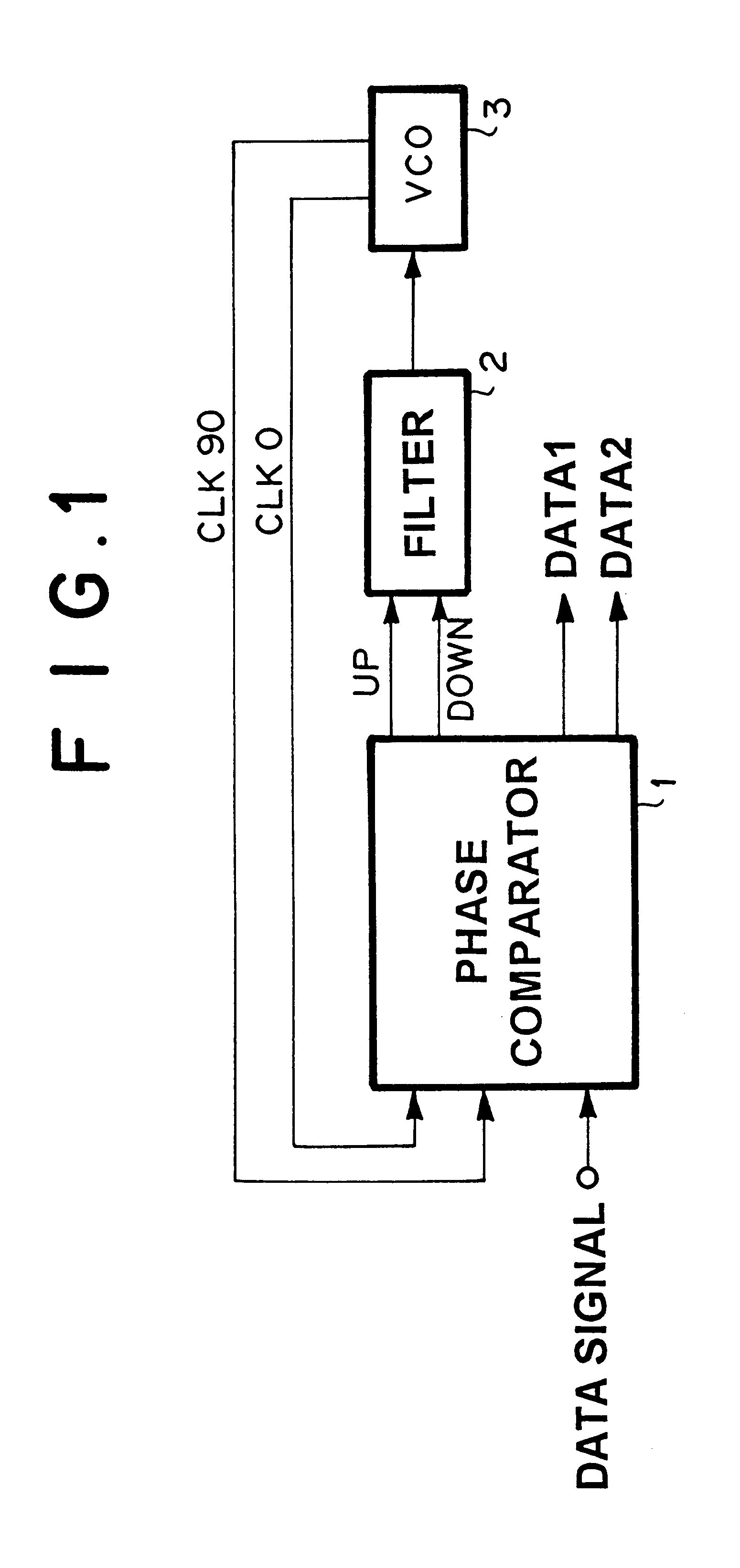
The first embodiment is shown in FIG. 1.

The inputs into phase comparator 1 are NRZ data signal, clock signal CLK0 of which frequency is a half of that of the NRZ data signal, and CLK90 of which phase is shifted by .pi. / 2, compared with CLK0. Here, CLK0 and CLK90 are outputted from VCO 3.

Phase comparator 1 outputs UP signal, when the clocks are delayed, compared with the NRZ data signal, while it outputs DOWN signal, when the clocks are advanced, compared with the NRZ data signal.

Filter 2 outputs a control voltage for raising the frequency of VCO 3 on the basis of the UP signal, while it outputs a control voltage for lowering the frequency of VCO 3.

VCO 3 outputs CLK0 and CLK90 on the basis of the output from filter 2.

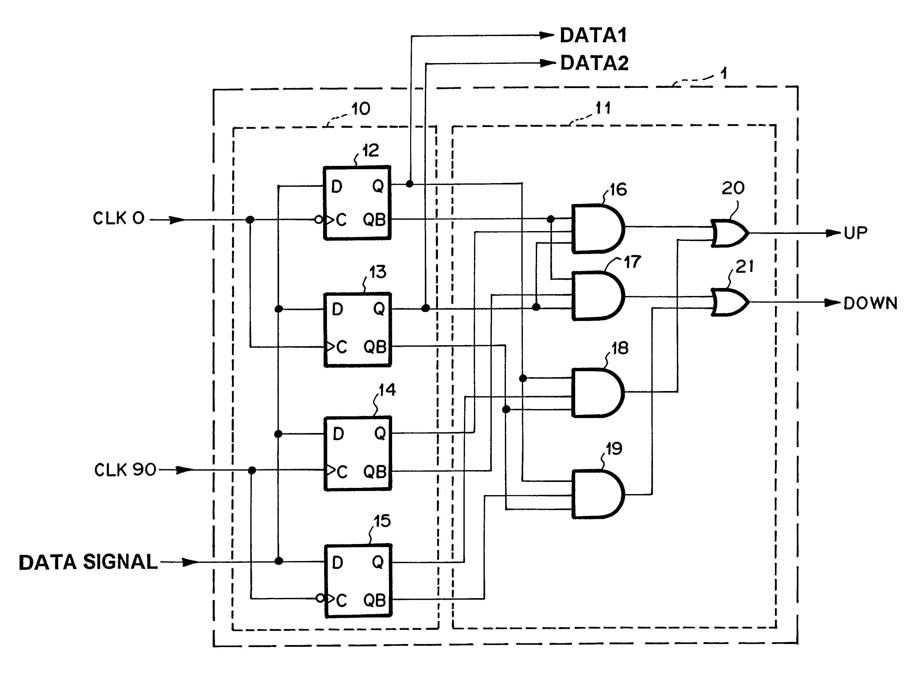
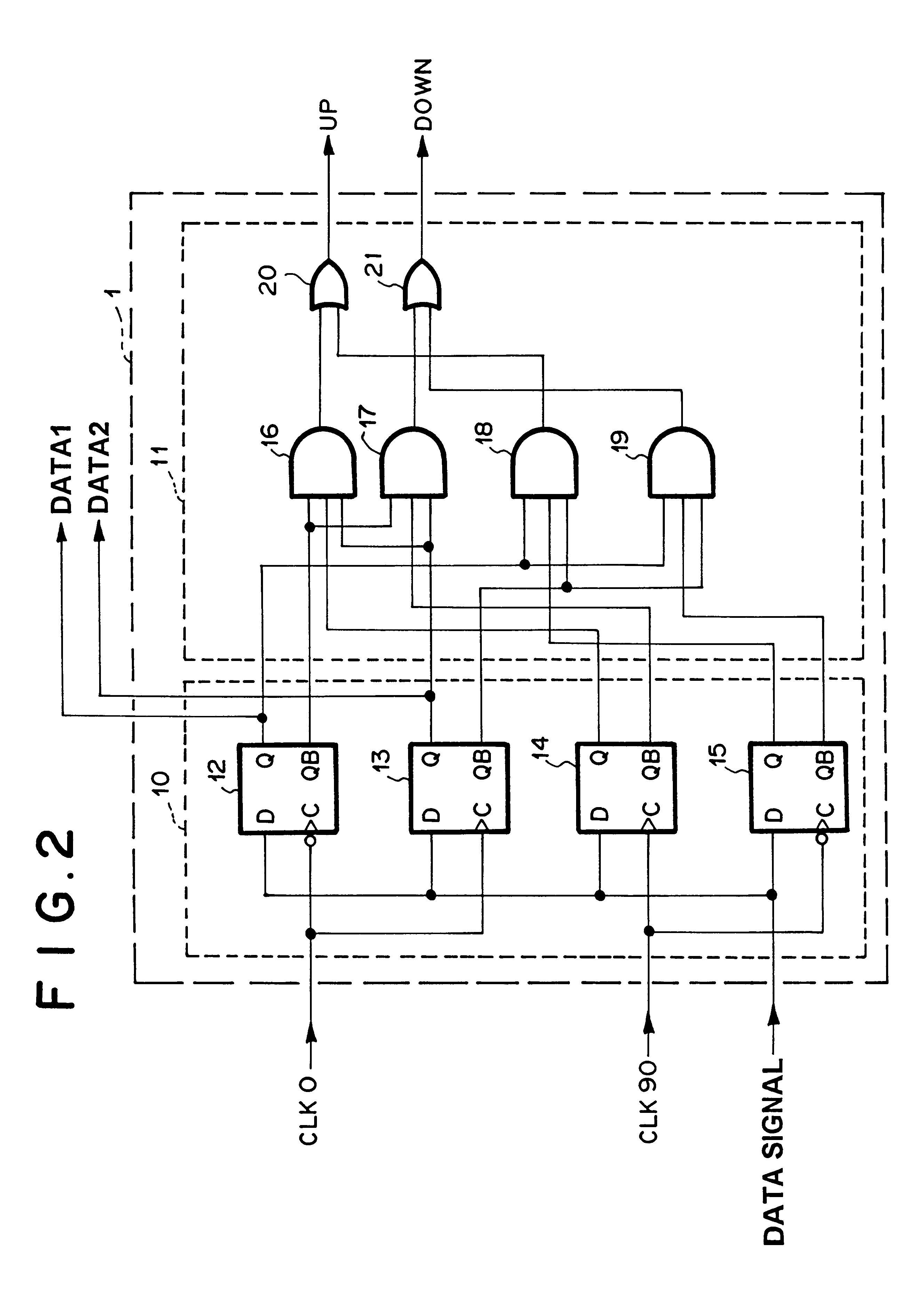
Phase comparator 1 as shown in FIG. 2 comprises sampling circuit 10, up down signal output circuit 11. Here, sampling circuit 10 comprises first determination means 12, second determination means 13, first DFF 14, and second DFF 15.

Further, in the first embodiment, first...

second embodiment

is shown in FIG. 4.

Phase comparator 1 comprises sampling circuit 10 and up-down signal output circuit 11, similarly to that as shown in FIG. 2. Further, sampling circuit 10 comprises first and second determination means 12 and 13, respectively, first and second DFFs 14 and 15, respectively. Up down signal output circuit 11 comprises first to fourth AND circuits 16 to 19, respectively, first and second OR circuits 20 and 21, respectively. The operations of sampling circuit 10 and up down signal circuit 11 are the same as those of sampling circuit 10 and up down signal circuit 11 as shown in FIG. 2.

The data input terminal D of third DFF 30 is connected with the output terminal of first OR circuit 20. The data input terminal D of fourth DFF 31 is connected with the output terminal of second OR circuit 21. CLK90 is inputted into the clock input terminal D of third and fourth DFFs 30 and 31, respectively. The UP signal is outputted from the output terminal Q of third DFF 30, while the DO...

third embodiment

is shown in FIG. 6.

First or second determination means 12 or 13, respectively, in sampling circuit 10 in phase comparator 1 in the third embodiment is shown in FIG. 6. First or second determination means 12 or 13, respectively, comprises first to third latches 40 to 42, respectively.

First to third latch circuits 40 to 42, respectively, latch data DD at the rise up of clock CC, hold the DD during the rise up and fall down of clock CC, and output inverted DD from the terminal O. First or second determination means 12 or 13, respectively, outputs a positive logic output Q from output terminal O of second latch 32, and also outputs an inverted logic output QB from output terminal O of third latch 33.

Determination means 12 latches the data signal at the fall down of the clock, while determination means 13 latches the data signal at the rise up of the clock. Therefore, the output Q from first determination means 12 and the output QB from second determination means 13 are outputted simulta...


PUM


Abstract

To provide a high speed digital PLL circuit which is easily manufactured by IC process. The phase of data signal is locked with a first clock of which frequency is the half of the data signal. Further, a second clock of which phase is shifted by pi/2 compared with the first clock is used for determining phase delay or phase advance of the data signal compared with the first clock. VCO outputs the first clock and the second clock. The phase comparator for inputting the data signal, the first and second clock, outputs a first data sampled at rise up of the first clock, a second data sampled at fall down of the first clock, a first indication signal indicating the phase delay, and a second indication signal indicating the phase advance. The filter for inputting the first and second indication signal outputs a control voltage for VCO.

Description

1. Technical Field of the InventionThe present invention relates to a high speed digital phase locked loop (PLL) circuit which is easily manufactured in the form of an integrated circuit (IC).2. Description of the Prior ArtRecently, various PLL circuits have been developed, because a clock recovery circuit using the PLL circuit is important for providing a small sized apparatus for data transmission.For example, a PLL circuit of which phase comparator comprises delay flip-flops (DFF) is disclosed in "A Monolithic 2,3-Gb / s 100 mV Clock and Data Recovery Circuit in Silicon Bipolar Technology" IEEE Journal of Solid--State Circuit. VOL.28, NO.12, pp. 1310-1313, December 1993.A conventional PLL circuit is shown in FIG. 7. The PLL circuit as shown in FIG. 7 comprises phase comparator 50, filter 51, voltage controlled oscillator (VCO) 52, and determination means 53. Further, phase comparator 50 comprises first DFF 54 and second DFF 55.The clock signal from VCO 52 is sampled by the data sig...

Claims


Application Information

Patent Timeline
Patent Type & Authority Patents(United States)
IPC IPC(8): H03L7/08H03L7/091H03L7/089H03D13/00H04L7/033H03K5/26
CPCH03D13/004H03L7/089H03L7/091H04L7/033G11C7/22H03L7/081H03L7/099
Inventor SODA, MASAAKI
Owner NEC ELECTRONICS CORP
Why Eureka
Try Eureka