Defective pixel compensation method

a pixel compensation and defect technology, applied in the field of defective pixel compensation, can solve the problems of limiting the resolution and accuracy available for optical imaging, limiting the line width and accuracy of printed patterns on workpieces, and affecting the quality of printed patterns

Inactive Publication Date: 2003-09-09
MICRONIC LASER SYST AB
View PDF11 Cites 151 Cited by
  • Summary
  • Abstract
  • Description
  • Claims
  • Application Information

AI Technical Summary

Problems solved by technology

For example a problem with Spatial Light Modulators is that one or a plurality of pixels in a given SLM may be defective, i.e. they may not respond to a control signal as intended.
These defective pixels in a computer controlled reticle may limiting the resolution and accuracy available for their use in optical imaging; e.g., the production of printed patterns on a workpiece may be limited as to its line widths and accuracy.

Method used


Image

  • Defective pixel compensation method
  • Defective pixel compensation method
  • Defective pixel compensation method

Examples


Embodiment Construction

Workpiece in the description below is meant to mean one of the group of: substrate for producing semiconductors (direct write), mask substrate, reticle substrate.

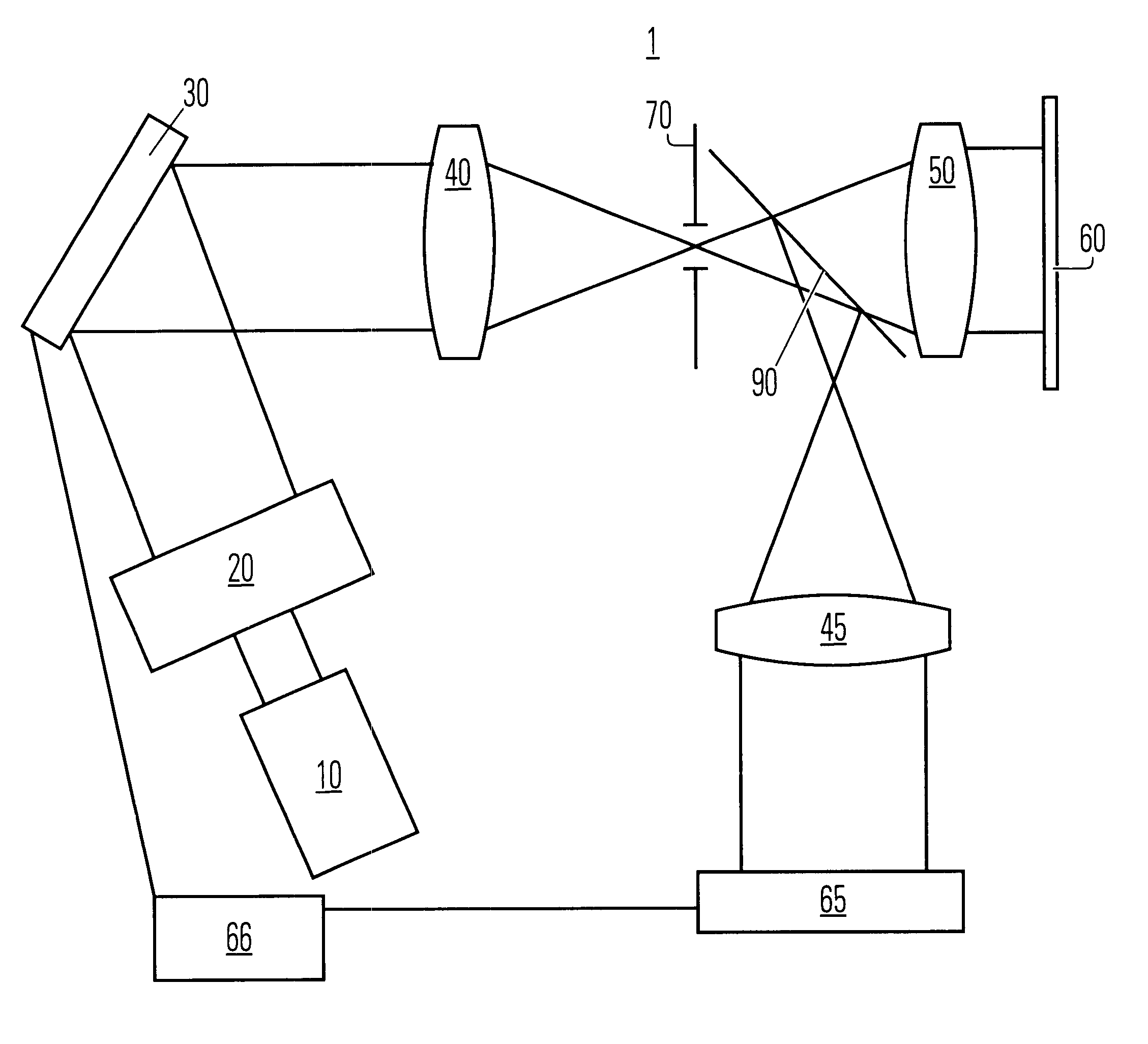
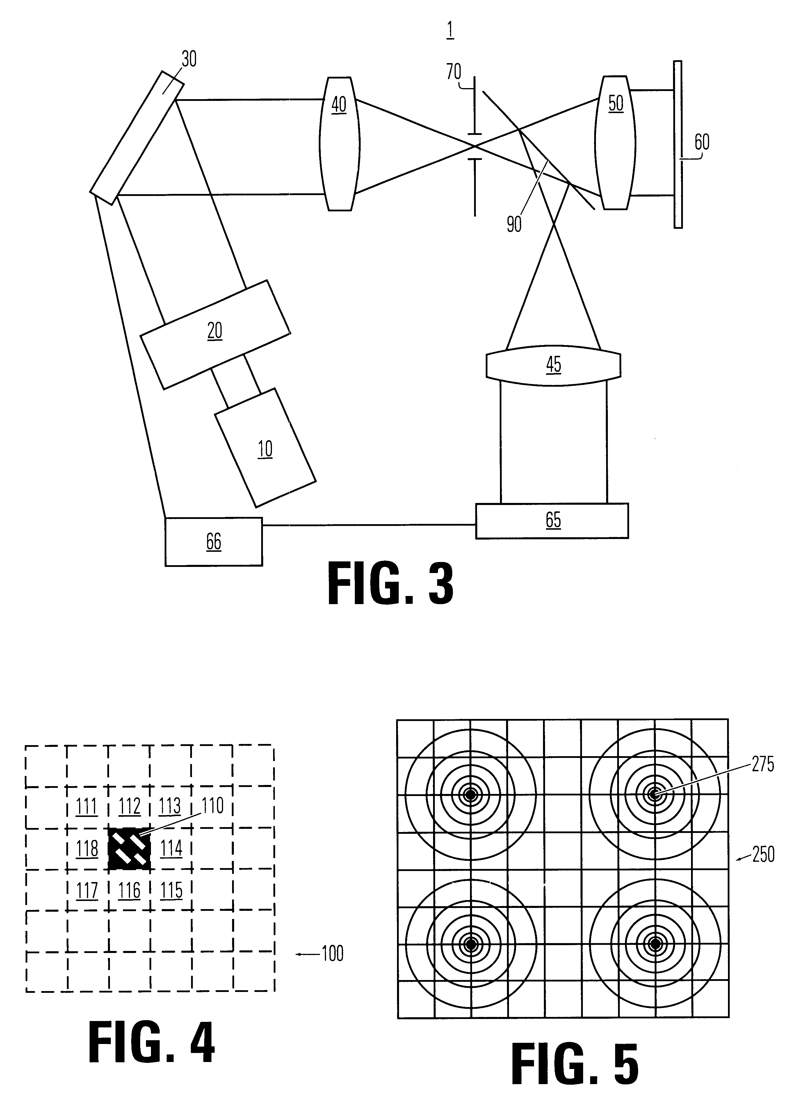
FIG. 3 illustrates an exemplary embodiment of an apparatus 1 for patterning a work piece 60. Said apparatus 1 comprising a source 10 for emitting electromagnetic radiation, a first lens arrangement 50, a computer controlled reticle 30, a beam conditioner arrangement 20, a spatial filter 70 in a Fourier plane, a third lens arrangement 40, a second lens arrangement 45, a beam splitter 90 and a detector arrangement 65, a computer 66.

The source 10 may emit radiation in the range of wavelength from infrared (IR), which is defined as 780 nm up to about 20 nm, to extreme ultraviolet (EUV), which in this application is defined as the range from 100 nm and down as far as the radiation is possible to be treated as electromagnetic radiation, i.e. reflected and focused by optical components. The source 10 emits radiation either pulsed ...


PUM

PropertyMeasurementUnit
wavelengthaaaaaaaaaa
pulse lengthaaaaaaaaaa

Abstract

The present invention relates to a method for compensating the impact of at least one defective pixel with a known position in a spatial light modulator (SLM) when creating a pattern of the SLM on a work piece covered with a layer sensitive to electromagnetic radiation. A source for emitting electromagnetic radiation is provided. Said radiation is illuminating said SLM having a plurality of modulating elements (pixels). In a writing pass an image of said modulator is projected on said work piece. A compensation for defective pixels in at least one other writing pass is performed. The invention also relates to an apparatus for performing said method.

Description

The present invention relates in general to techniques for obtaining improved images by compensation methods. In particular it relates to a method for compensating defective pixels in a Spatial Light Modulator (SLM), used in optical lithography. It also relates to an apparatus for patterning a work piece comprising such a method and a method for detecting defective pixels.DESCRIPTION OF THE BACKGROUND ARTLithographic production is useful for integrated circuits, masks, reticles, flat panel displays, micro-mechanical or micro-optical devices and packaging devices, e.g. lead frames and MCM's. Lithographic production may involve an optical system to image a master pattern from a computer-controlled reticle onto a workpiece. A suitable workpiece may comprise a layer sensitive to electromagnetic radiation, for example visible or non-visible light. An example of such a system is described in WO 9945435 with the same inventor and applicant as the present invention.Said computer controlled ...

Claims


Application Information

Patent Timeline
Patent Type & Authority Patents(United States)
IPC IPC(8): G03F7/20G02F1/13H01L21/027
CPCG03F7/70291G03F7/70425G03F7/20G02B26/00
Inventor SANDSTROM, TORBJORN
Owner MICRONIC LASER SYST AB
Why Eureka
Try Eureka