Method for forming a capacitor of a semiconductor device

a technology of semiconductor devices and capacitors, which is applied in the direction of capacitors, semiconductor devices, electrical equipment, etc., can solve the problems of inability to reduce the thickness of effective oxide films, the inability to obtain capacitor capacitance sufficient for stable operation of devices, and the inability to form effective oxide films consisting of tantalum oxides having a thickness of 30 .ang. or less, so as to improve the film quality and improve the effect of characteristics

Inactive Publication Date: 2003-10-14
SK HYNIX INC
View PDF2 Cites 0 Cited by
  • Summary
  • Abstract
  • Description
  • Claims
  • Application Information

AI Technical Summary

Benefits of technology

Accordingly, a method for forming a capacitor of a semiconductor device is disclosed wherein a Ru film is formed using a CVD method at high temperature, which provides capacitor with improved film quality and characteristics during the subsequent process.
The Ru film is stacked at a high temperature ranging from about 300 to about 400.degree. C., preferably from 300 to 350.degree. C. to decrease RMS, which prevents the agglomeration phenomenon generated during the annealing process, improves quality of Ru film, minimizes oxygen content in the Ru films and inhibits formation of oxide film on the interface between Ru film and barrier metal layer, thereby improving the characteristics of the capacitors.

Problems solved by technology

However, the capacitance of semiconductor devices is proportional to the surface area of storage electrode and it became difficult to obtain capacitance of capacitor sufficient for stable operation of devices.
As a result, the thickness of the Ta.sub.2 O.sub.5 film is increased, the thickness T.sub.ox of effective oxide film cannot be reduced.
This makes it impossible to form an effective oxide film consisting of tantalum oxide having a thickness of about 30 .ANG. or less.
Here, the oxygen atoms included in the Ru film during the annealing process oxidize the interface of the barrier metal layer in the subsequent process of forming tantalum oxide films, thereby forming an oxide film, which results in degradation of electrical characteristics of capacitors of semiconductor devices and lift-off of Ru films.
As described above, the conventional method for forming a capacitor of a semiconductor device has a problem in degradation of electrical characteristics of devices due to oxygen contained in Ru films.
Also, Ru films stacked at a temperature of 260.degree. C. have low quality of film, thereby generating an agglomeration phenomenon during the subsequent annealing process to expose barrier metal layers.

Method used


Image

  • Method for forming a capacitor of a semiconductor device
  • Method for forming a capacitor of a semiconductor device
  • Method for forming a capacitor of a semiconductor device

Examples


Embodiment Construction

A disclosed method for forming a capacitor of a semiconductor device will be described in detail referring to the accompanying drawings.

FIGS. 4a to 4g are cross-sectional diagrams illustrating a method for forming a capacitor of a semiconductor device in accordance with a preferred embodiment wherein the capacitor is a cylinder-type capacitor.

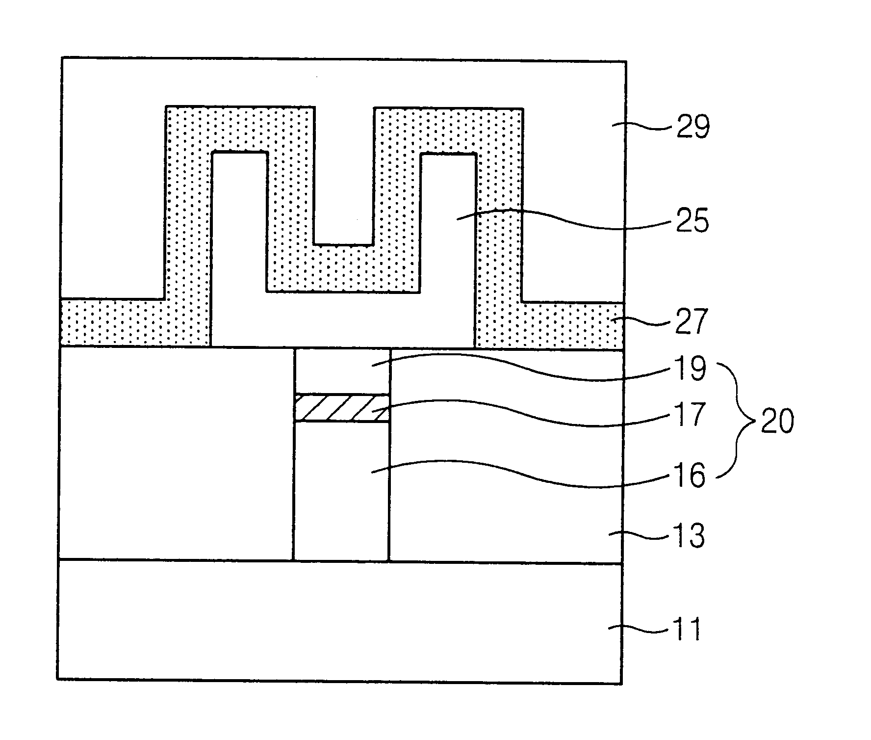
Referring to FIG. 4a, a lower insulating layer 13 is sequentially formed on the substrate 11 which comprises a device isolation film (not shown), a word line (not shown) and a bit line (not shown), and has a planarized top surface.

The lower insulating layer 13 comprises insulating materials having high fluidity such as BPSG (borophosphosiicate glass), PSG (phosphosilicate glass), FSG (fluorosilicate glass), PE-TEOS (plasma enhanced-tetraethoxysilicate glass), PE-SiH.sub.4 (plasma enhanced-silane), HDP USG (high density plasma undoped silicate glass), HDP PSG (high density plasma phosphosilicate glass) and combinations thereof.

Thereafter, the lo...


PUM

PropertyMeasurementUnit
temperatureaaaaaaaaaa
pressureaaaaaaaaaa

Abstract

Methods for forming capacitors of semiconductor devices, and more specifically, to a method for forming a capacitor having a stacked structure of metal layer-insulating film-metal layer and having its storage electrode formed of ruthenium (hereinafter, referred to as 'Ru') and dielectric layer formed of tantalum oxide (Ta<HIL><PDAT>2< / SB><PDAT>O<HIL><PDAT>5< / SB><PDAT>) film, which provides improved formation of dense Ru film using a CVD method at high temperature, thereby improving electrical characteristics of the capacitor.< / PTEXT>

Description

1. Technical FieldMethods for forming capacitors of semiconductor devices are disclosed, and more specifically, methods are disclosed for forming capacitors having a stacked structure of metal layer-insulating film-metal layer and having its storage electrode formed of ruthenium (hereinafter, referred to as `Ru`) and dielectric layer formed of tantalum oxide (Ta.sub.2 O.sub.5) film, which provides improved formation of dense Ru film using a CVD method at high temperature, thereby improving electrical characteristics of the capacitor.2. Description of the Related ArtCurrently, due to high integration of semiconductor devices, the cell size becomes smaller and the surface area of storage electrode is decreased. However, the capacitance of semiconductor devices is proportional to the surface area of storage electrode and it became difficult to obtain capacitance of capacitor sufficient for stable operation of devices.Specifically, in case of high integration of DRAM device having a uni...

Claims


Application Information

Patent Timeline
Patent Type & Authority Patents(United States)
IPC IPC(8): H01L21/285H01L21/02H01L21/316H01L21/8242
CPCH01L21/28556H01L28/60H01L21/31604H01L27/10855H01L28/91H01L28/65H01L28/55H01L21/02323H01L21/02197H01L21/02183H10B12/0335H10B99/00H01L21/0234H01L21/02348
Inventor KIM, KYONG MINSUN, HO-JUNG
Owner SK HYNIX INC
Why Eureka
Try Eureka