Thin film piezoelectric resonator

a piezoelectric resonator and thin film technology, applied in piezoelectric/electrostrictive devices, piezoelectric/electrostrictive/magnetostrictive devices, piezoelectric/electrostriction/magnetostriction machines, etc., can solve the problems of reducing the mass of the cover layer, expensive lithography, etc., and achieve high accuracy

Inactive Publication Date: 2003-12-02
AVAGO TECH INT SALES PTE LTD
View PDF16 Cites 167 Cited by
  • Summary
  • Abstract
  • Description
  • Claims
  • Application Information

AI Technical Summary

Benefits of technology

The object of the invention is to provide a thin film piezoelectric resonator which overcomes the above-noted deficiencies and disadvantages of the prior art devices and methods of this kind, and which can be set to a prescribed resonant frequency using simple means and with high accuracy. It is a further object to specify how a plurality of resonant frequencies can be set in a simple way.
In accordance with another feature of the invention, the structure is defined in such irregular distribution and dimensioning that diffraction phenomena are avoided.
In summary, the thin film piezoelectric resonator of the invention has, in the layer of the cover electrode, or in an additional layer specifically applied therefor, holes, preferably produced lithographically, or similar structures. The structures have a mean spacing from one another which is smaller than the acoustic wavelength provided during operation of the component. These structures are preferably distributed with a uniformity that is sufficient to effect a uniform change in the mass of the layer per area (area density), thus producing a specific setting of the resonant frequency / frequencies. On the other hand, the structures are preferably distributed so irregularly that diffraction effects are avoided.

Problems solved by technology

The resonant frequency of thin film piezoelectric resonators can basically be trimmed by applying additional layers, as described above, but this necessitates expensive lithography.
Material can be removed over the entire surface by laser trimming or ion-beam trimming, and this reduces the mass of the cover layer, although necessitating an expensive fabrication step at the end of the fabrication process.

Method used


Image

  • Thin film piezoelectric resonator
  • Thin film piezoelectric resonator
  • Thin film piezoelectric resonator

Examples


Embodiment Construction

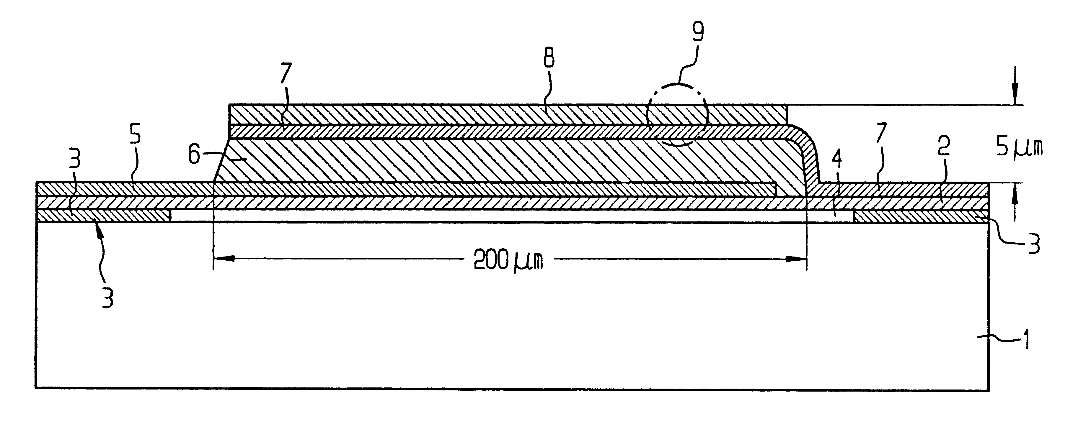
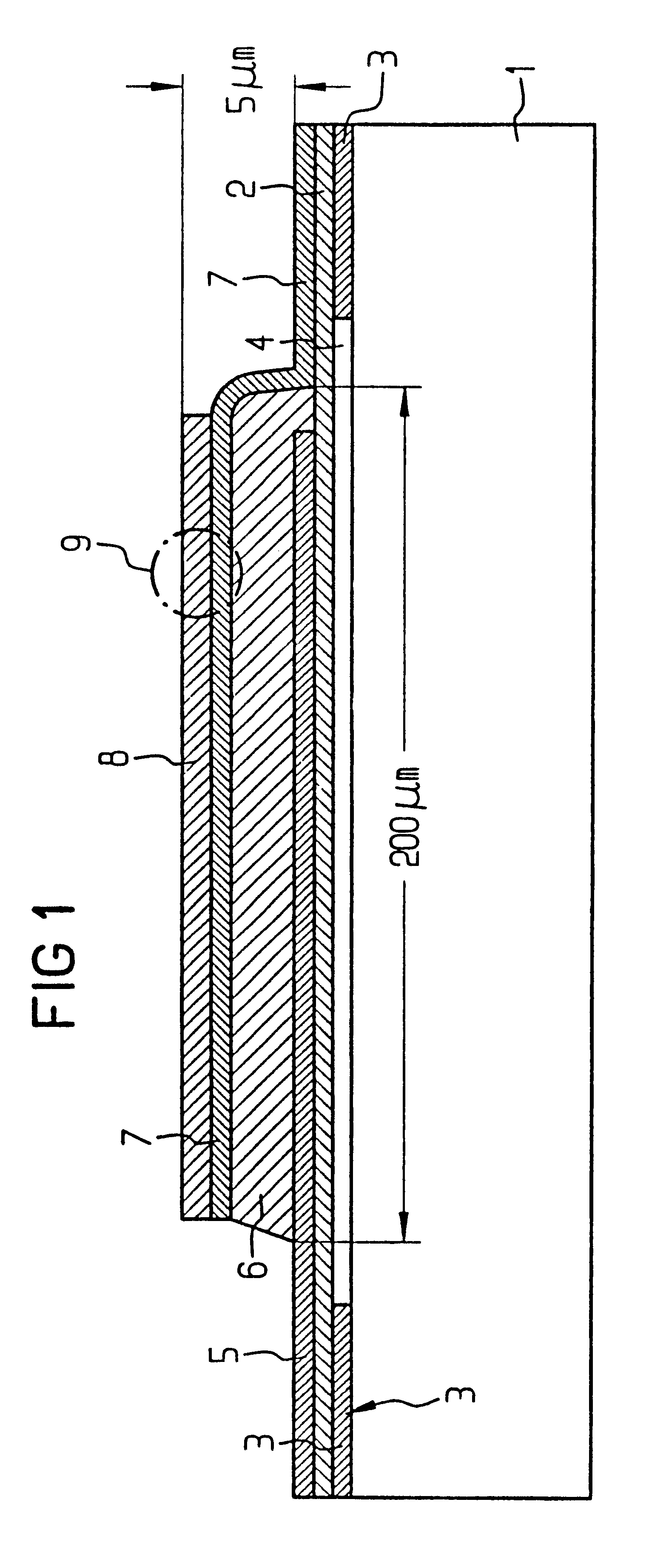
Referring now to the figures of the drawing in detail and first, particularly, to FIG. 1 thereof, there is seen an exemplary resonator according to the invention, in cross section. A carrier film 2 is located on a substrate 1. The carrier film 2 is preferably formed of polysilicon. A cavity 4 in an auxiliary layer 3, for example made from oxide, is disposed below the carrier film 2. The cavity 4 is located in the region of a layer structure provided as resonator. The cavity typically has the illustrated dimension of approximately 200 .mu.m. The layer structure of the resonator is located on the carrier film 2. The layer structure comprises a lower electrode layer 5 provided for the bottom electrode, a piezoelectric layer 6, and an upper electrode layer 7 provided for the cover electrode. The electrode layers 5, 7 are preferably metal, and the piezoelectric layer 6 is, for example, AlN, ZnO, or PZT ceramic (PbZrTi). This layer structure overall typically has the illustrated thickness...


PUM


Abstract

The layer of the cover electrode, or an additional layer on the cover electrode is formed with holes, preferably produced lithographically, or similar structures. The structures have a mean spacing from one another which is smaller than the wavelength for operating the component. The structures are preferably distributed with a uniformity sufficient to effect a uniform change in the mass of the layer per area, thus producing a specific setting of the resonant frequency / frequencies, and are preferably, on the other hand, distributed so irregularly that diffraction effects are avoided.

Description

1. Field of the InventionThe present invention relates to a thin film piezoelectric resonator which can be produced using micromechanical methods.The resonant frequency of thin film piezoelectric resonators in the frequency range above 500 MHz is indirectly proportional to the layer thickness of the piezoelectric layer. The carrier membrane and the bottom and cover electrodes constitute an additional mass loading for the resonator which effects a reduction in the resonant frequency. The thickness fluctuations in all these layers determine the range of manufacturing tolerances in which the resonant frequency of a specimen resonator lies. Layer thickness fluctuations of 5% are typical for sputtering processes in microelectronics. A 1% tolerance can be achieved with a considerable outlay. Fluctuations occur both statistically from wafer to wafer and systematically between the middle of the wafer and the edge. The resonant frequencies of individual resonators must exhibit an absolute ac...

Claims


Application Information

Patent Timeline
Patent Type & Authority Patents(United States)
IPC IPC(8): H03H9/17H03H3/04H03H9/00H03H3/00H03H9/02
CPCH03H3/04H03H9/173H03H2003/0428
Inventor AIGNER, ROBERT
Owner AVAGO TECH INT SALES PTE LTD
Why Eureka
Try Eureka