Logic power optimization algorithm

a logic network and power optimization technology, applied in the field oflogic networks, can solve the problems of large amount of ac power cmos circuit designs consume, waste of considerable power in typical cmos logic network designs, and useless internal nodes

Inactive Publication Date: 2003-12-02
GOOGLE LLC
View PDF10 Cites 22 Cited by
  • Summary
  • Abstract
  • Description
  • Claims
  • Application Information

AI Technical Summary

Problems solved by technology

Nonetheless, as the size and complexity of CMOS integrated circuits continue to grow, a need still exists to eliminate the fairly large amount of AC power CMOS circuit designs consume.
In particular, considerable power is wasted in typical CMOS logic network designs because internal nodes toggle uselessly, calculating outputs which are frequently unneeded.
This thought process leads to many nodes within the network toggling when, in fact, they are doing no useful work.
Thus, present design and synthesis methods for CMOS logic result in considerable wasted power because portions of the logic network are allowed to toggle even when the outputs from these portions are unneeded and unused.
Therefore, without some system of eliminating unnecessary toggling of gates in a CMOS circuit, digital logic designs will continue to consume unnecessarily high amounts of AC power.
Those logic groups that do not contribute to the desired output, will nonetheless be a drain on the power to the network.

Method used


Image

  • Logic power optimization algorithm
  • Logic power optimization algorithm
  • Logic power optimization algorithm

Examples


Embodiment Construction

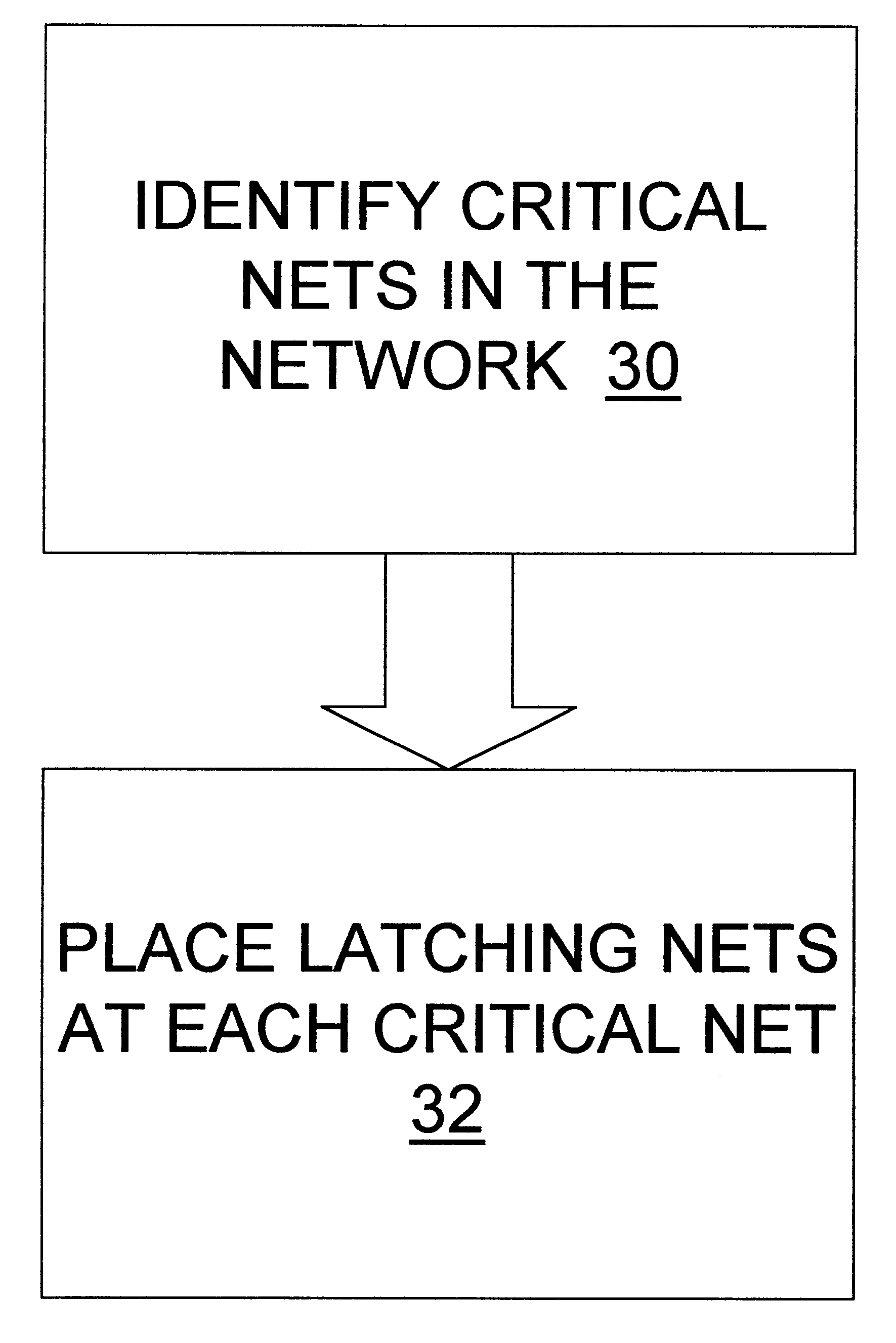
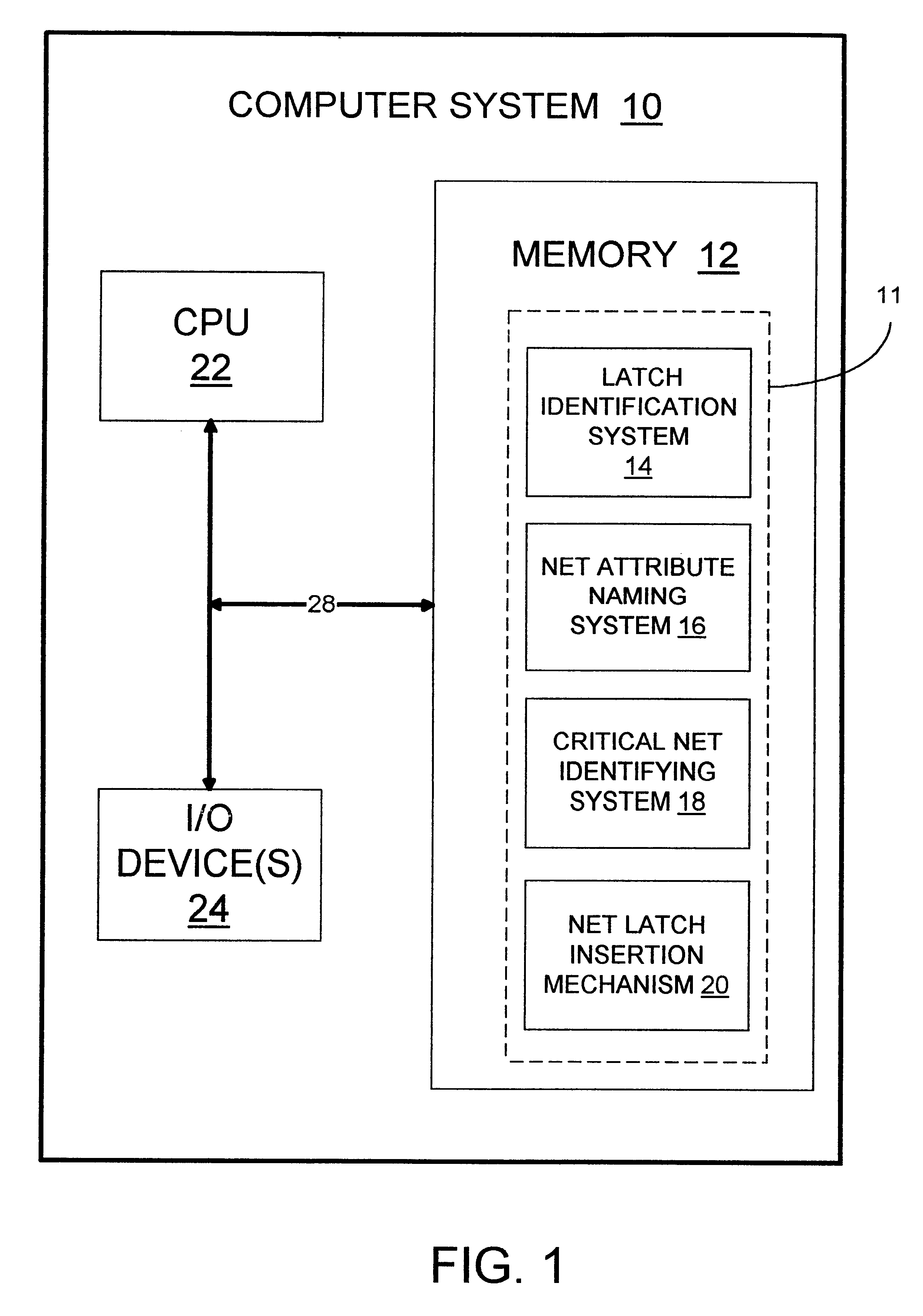
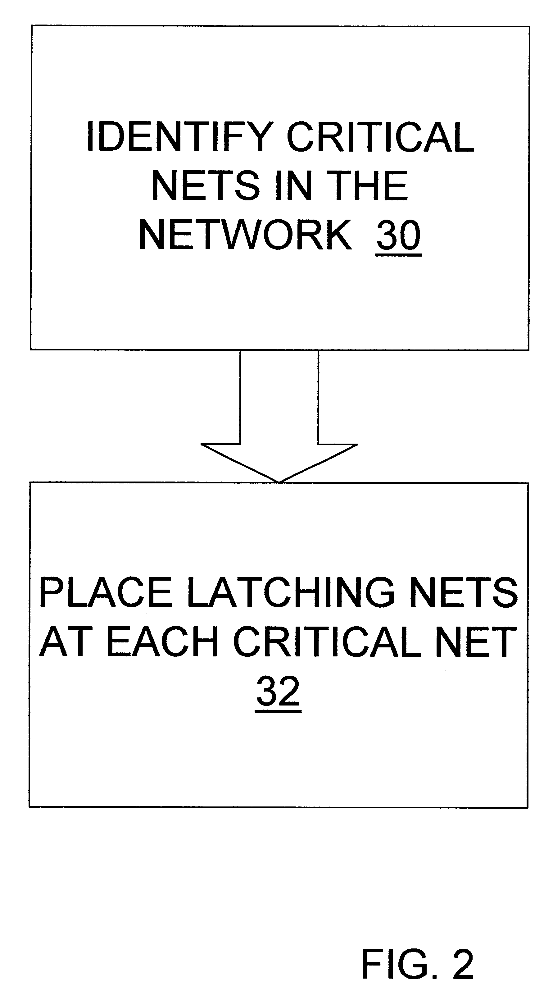
Referring now to the drawings, FIG. 1 depicts a computer system 10 having a central processing unit (CPU) 22, input / output (I / O) devices 24, bus 28 and memory 12. It is recognized that computer system 10 may include additional components and / or may have its components residing in different physical locations on different physical devices. Memory 12 is shown containing a software program 11 comprised of 4 modules. Memory 12 may be implemented by any known type of memory system capable of holding software programs, such as a hard drive, an optical disk, RAM, ROM, a transmission medium, magnetic tape and / or magnetic disks. Computer software program 11 is shown including a latch identification system 14, a net attribute naming system 16, a critical net identifying system 18, and a latching net insertion mechanism 20.

Latch identification system 14 includes a system for identifying and grouping all enabled latches, wherein each of the enabled latches comprises a first input for receiving ...


PUM


Abstract

Disclosed is a system and method for eliminating the unnecessary toggling of logic in a logic network. The method and system can be incorporated directly into logic synthesis software, or may be implemented manually. Provided is a mechanism for identifying critical nets and then inserting net latches at the critical nets wherein each net latch is controlled by an enable signal that also controls a related output latch. Each net latch is comprised of a circuit which can on command hold static the last logic level on a given logic node.

Description

1. Field of the InventionThe present invention relates to logic networks, and more particularly to a system and method for eliminating the unnecessary toggling of nodes in the logic network.2. Related ArtComplimentary Metal Oxide Semiconductor (CMOS) technology is now universally applied in digital logic circuits. CMOS devices are fabricated to provide either a high or low output level (e.g., 0 or 5 volts) while drawing very little power from the power supply. Moreover, CMOS circuitry includes the advantage of nearly eliminating DC power. Nonetheless, as the size and complexity of CMOS integrated circuits continue to grow, a need still exists to eliminate the fairly large amount of AC power CMOS circuit designs consume.In particular, considerable power is wasted in typical CMOS logic network designs because internal nodes toggle uselessly, calculating outputs which are frequently unneeded. In most current logic designs, the focus is on making sure the logic path is functionally corr...

Claims


Application Information

Patent Timeline
Patent Type & Authority Patents(United States)
IPC IPC(8): G06F17/50
CPCG06F17/5022G06F17/505G06F2217/78G06F30/327G06F30/33G06F2119/06G06F30/3308
Inventor GOODNOW, KENNETH J.MICHAIL, MICHEL S.OGILVIE, CLARENCE R.PRICER, WILBUR D.VENTRONE, SEBASTIAN T.
Owner GOOGLE LLC
Why Eureka
Try Eureka