Semiconductor integrated circuit and IC card

a technology of integrated circuit and ic card, which is applied in the direction of static storage, digital storage, instruments, etc., can solve the problems of sub-threshold leakage and waste of power consumption, and achieve the effects of preventing the production of relatively large noise, reducing the speed of operation of reading data out of the memory, and enhancing the discharge ra

Inactive Publication Date: 2006-07-27
HITACHI ULSI SYST CO LTD +1
View PDF5 Cites 0 Cited by
  • Summary
  • Abstract
  • Description
  • Claims
  • Application Information

AI Technical Summary

Benefits of technology

[0011] The technology disclosed in Patent Document 2 is that the bit lines and source lines of memory cells unselected for access when a memory is active are brought to a bit line potential. With this technology, wasteful power consumption in active state can be reduced; however, there is the possibility that the access rate may be lowered. More specifically, source lines which transition from a state of unselected for access to a state of selected for access must be discharged before readout operation is started. The cycle of readout operation is lengthened by a time for which it waits for the completion of the discharge operation.
[0040] If the potential of the source lines is made equal to the precharge potential of the bit lines on standby, the source lines are discharged in response to an instruction to transition from standby state to active state. Then, the current supplying capability thereof is varied so that the discharge rate will be enhanced stepwise. Thus, currents are prevented from concentratedly flowing from a large number of memory cells to the source lines at a time. As a result, the production of relatively large noise is prevented.

Problems solved by technology

Therefore, wasteful power consumption due to sub-threshold leakage occurs even in standby state as long as a potential difference is produced between the source and drain of a memory cell by bit line precharge.

Method used


Image

  • Semiconductor integrated circuit and IC card
  • Semiconductor integrated circuit and IC card
  • Semiconductor integrated circuit and IC card

Examples


Embodiment Construction

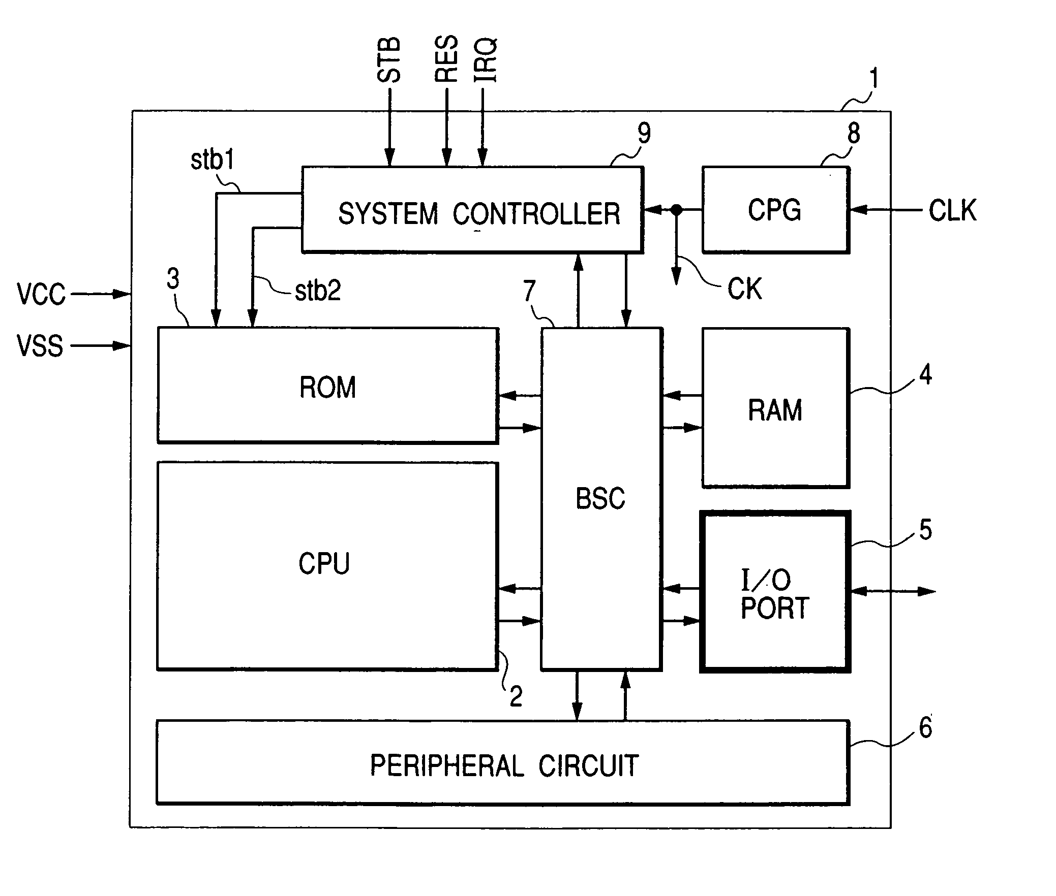
[0068]FIG. 1 illustrates a microcomputer as an example of the semiconductor integrated circuit according to the present invention. The microcomputer 1 illustrated in the figure is formed on a semiconductor substrate (semiconductor chip) of single crystal silicon or the like, for example, by CMOS integrated circuit manufacturing technology. The microcomputer 1 receives supply voltage VCC and the ground voltage VSS of the circuit as operating power supply.

[0069] The microcomputer 1 comprises a central processing unit (CPU) 2, a read only memory (ROM) 3 which holds operating programs and the like for the CPU 2; a random access memory (RAM) 4 used as a work area for the CPU 2 or for like purposes; I / O ports 5 connected with an external bus and the like; a peripheral circuit 6 of a timer and the like; a bus controller (BSC) 7, a clock pulse generator (CPG) 8, and a system controller 9.

[0070] The CPU 2 comprises an instruction control part which decodes instructions fetched from the ROM...


PUM


Abstract

A semiconductor integrated circuit has a memory which can enter active state or standby state, and the memory has voltage generation circuits for bit lines and source lines with which memory cells are connected. The voltage generation circuits make the potential of the bit lines and the potential of the source lines equal to each other in response to an instruction to transition from active state to standby state. The voltage generation circuits produce a potential difference between the bit lines and the source lines in response to an instruction to transition from standby state to active state. In standby state, the potential of the bit lines and that of the source lines are equal to each other. Therefore, sub-threshold leakage does not occur between the source and drain of each memory cell. In active state, the source line potential is not varied.

Description

CROSS-REFERENCE TO RELATED APPLICATION [0001] This application is a Continuation Application of U.S. application Ser. No. 10 / 748,137 filed on Dec. 31, 2003. Priority is claimed based upon U.S. application Ser. No. 10 / 748,137 filed on Dec. 31, 2003, which claims the priority dates of Japanese Patent Application Nos. 2003-016573 and 2003-370078 filed on Jan. 24, 2003 and Oct. 30, 2003, respectively, the entire contents of which is incorporated herein by reference.BACKGROUND OF THE INVENTION [0002] The present invention relates to a semiconductor integrated circuit provided with a memory and more particularly to a technology for reducing leakage currents in memory cells in low-power consumption state, such as standby state, which is applicable to, for example, a microcomputer provided with a large-capacity ROM. [0003] There is a technology for reducing power consumption and yet preventing increase in access delay. According to this technology, the substrate bias voltage of a peripheral...

Claims


Application Information

Patent Timeline
Patent Type & Authority Applications(United States)
IPC IPC(8): G11C5/14G11C17/00G11C5/00G11C7/00G11C7/12G11C7/22G11C11/4063G11C11/409G11C17/12G11C17/18
CPCG11C5/14G11C7/12G11C7/22G11C17/12G11C2207/2227
Inventor TAKAZAWA, YOSHIOYAMADA, TOSHIOOZAWA, SHINICHIKANAI, TAKEOKATOH, MINORUYAMAUCHI, KOUDOUARAKI, TOSHIHIRO
Owner HITACHI ULSI SYST CO LTD
Why Eureka
Try Eureka