Correction of birefringence in cubic crystalline optical systems

a cubic crystalline optical system and birefringence technology, applied in the field of birefringence correction in cubic crystalline optical systems, can solve the problems of different wavefront aberrations, degrade image resolution, introduce field distortion, and optical path difference or retardance, etc., to achieve the effect of reducing retardan

Inactive Publication Date: 2004-01-27
ASML NETHERLANDS BV
View PDF17 Cites 57 Cited by
  • Summary
  • Abstract
  • Description
  • Claims
  • Application Information

AI Technical Summary

Problems solved by technology

When light passes through a unit length of a birefringent material, the difference in refractive index for the two ray paths will result in an optical path difference or retardance.
Each of the orthogonal wavefronts will experience a different refractive index, resulting in different wavefront aberrations.
When used for construction of elements of an optical system, the birefringent properties of these cubic crystalline materials may produce wavefront aberrations that significantly degrade image resolution and introduce field distortion.

Method used


Image

  • Correction of birefringence in cubic crystalline optical systems
  • Correction of birefringence in cubic crystalline optical systems
  • Correction of birefringence in cubic crystalline optical systems

Examples


embodiment 1

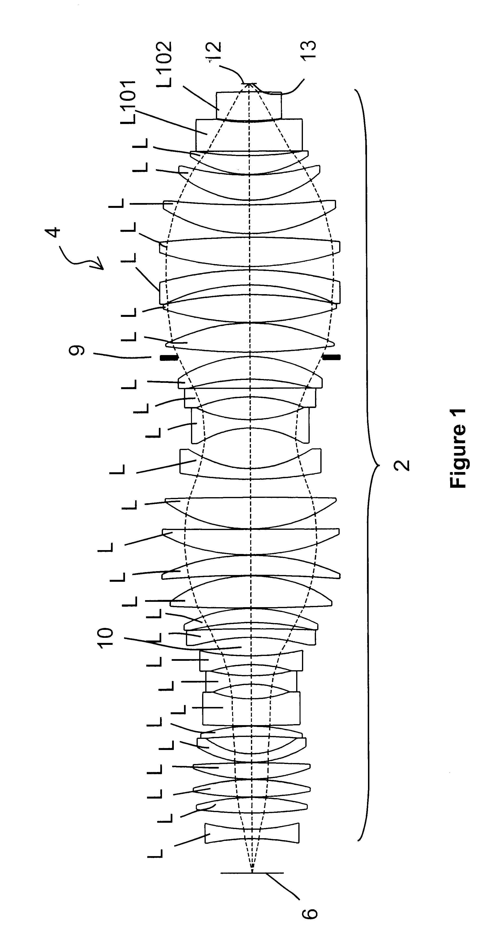
This embodiment may be applied to the exemplary optical system shown in FIG. 6. In embodiment 1 of the present invention, the first two elements 46 and 44 are oriented along the [110] cubic crystalline lattice direction and the third element 42 is oriented along the [100] lattice direction, although the specific order of the elements may be varied in other exemplary embodiments. Furthermore, the crystal lattices of the [110] first 46 and second 44 elements are rotated by 90 degrees with respect to one another in a plane perpendicular to the optical axis. This rotation about the optical axis is known as "clocking".

FIGS. 8A, 8B, and 8C are graphical illustrations showing the retardance magnitude and orientation over the pupil for the individual elements in the arrangement of the first exemplary embodiment of the optical system shown in FIG. 6, as described above. FIGS. 8A, 8B and 8C represent the individual retardance contributions for the first 46, second 44, and third 42 cubic cryst...

first embodiment

According to another exemplary embodiment, the residual error in FIG. 9B may be further reduced by a birefringent element that produces radially-oriented retardance that increases in magnitude from the center to the edge of the component. Such an element may be produced by applying a hoop stress to the edge of a meniscus optical component and added to the exemplary optical system of the first embodiment and as shown in FIG. 6. The applied stress creates a spatially varying birefringence to compensate for the computed or measured birefringence variation within the optical system as shown in FIG. 9B. Various stresses may be applied to various optical elements to achieve the spatially varying birefringence. The stressed optical element may be a lens element or a window and aligned along the optical axis. Various techniques may be used to apply the stress.

FIG. 9D shows the spatial radial retardance variation induced by applying an exemplary compressive hoop stress of 1000 pounds per squ...

embodiment 2

According exemplary embodiment 2, the present invention provides an apparatus that achieves reduced retardance through the use of at least four [110] optical elements and at least one [100] optical element. In the illustrated embodiment shown in FIG. 10, the present invention provides an apparatus having four elements with their [110] crystal axes along the system optical axis and one element with its [100] crystal axis along the system optical axis.

The relative orientations of the lattice directions in the plane perpendicular to the optical axis may be adjusted for the [110] optical elements. This technique is known as "clocking" or rotating the crystal lattice orientation of elements aligned along a common optical axis. The relative orientations may be selected in a particular manner that relates to the azimuthal orientations of the off-axis peak birefringence lobes.

Referring to FIG. 4, there are peak birefringence lobes at 60.degree. with respect to the [110] crystal axis, corres...


PUM

PropertyMeasurementUnit
wavelengthaaaaaaaaaa

Abstract

An optical system includes multiple cubic crystalline optical elements aligned along a common optical axis and having their crystal lattices oriented with respect to each other to minimize the effects of intrinsic birefringence and produce a system with reduced retardance. The optical system may be a refractive or catadioptric system having a high numerical aperture and using light with a wavelength at or below 248 nanometers. The net retardance of the system is less than the sum of the retardance contributions of the respective optical elements as the elements are oriented such that the intrinsic birefringences of the individual elements cancel each other out. In one embodiment, two [110] cubic crystalline optical elements are clocked with respect to one another and used in conjunction with a [100] cubic crystalline optical element to reduce retardance. Various birefringent elements, wave plates, and combinations thereof provide additional correction for residual retardance and wavefront aberrations. The optical system may be used in a photolithography tool to pattern substrates such as semiconductor substrates and thereby produce semiconductor devices.

Description

The present invention relates, most generally, to high performance optical systems and lithography methods. More particularly, the present invention relates to an apparatus and method for compensating for the effects of intrinsic birefringence in optical systems using cubic crystalline optical elements.In order to increase levels of device integration for integrated circuit and other semiconductor devices, there is a drive to produce device features having smaller and smaller dimensions. In today's rapidly advancing semiconductor manufacturing industry, there is a related drive to produce such device features in a reliable and repeatable manner.Optical lithography systems are commonly used in the fabrication process to form images of device patterns upon semiconductor substrates. The resolving power of such systems is proportional to the exposure wavelength; therefore, it is advantageous to use exposure wavelengths that are as short as possible. For sub-micron lithography, deep ultr...

Claims


Application Information

Patent Timeline
Patent Type & Authority Patents(United States)
IPC IPC(8): G02B27/28G03F7/20G02B13/24G02B17/08H01L21/027
CPCG02B1/02G02B27/0043G02B27/28G03F7/70075G03F7/70216G03F7/70241G03F7/70966Y10S438/942G02B13/24
Inventor HOFFMAN, JEFFREY M.MCGUIRE, JAMES P.
Owner ASML NETHERLANDS BV
Why Eureka
Try Eureka