Expandable slave device system
a slave device and slave technology, applied in the field of expandable slave device systems, can solve the problems of inability to achieve 100% bus utilization, data slot considered unused and wasted, and system of fig. 19a cannot achieve 100% bus utilization
- Summary
- Abstract
- Description
- Claims
- Application Information
AI Technical Summary
Benefits of technology
Problems solved by technology
Method used
Image
Examples
first embodiment
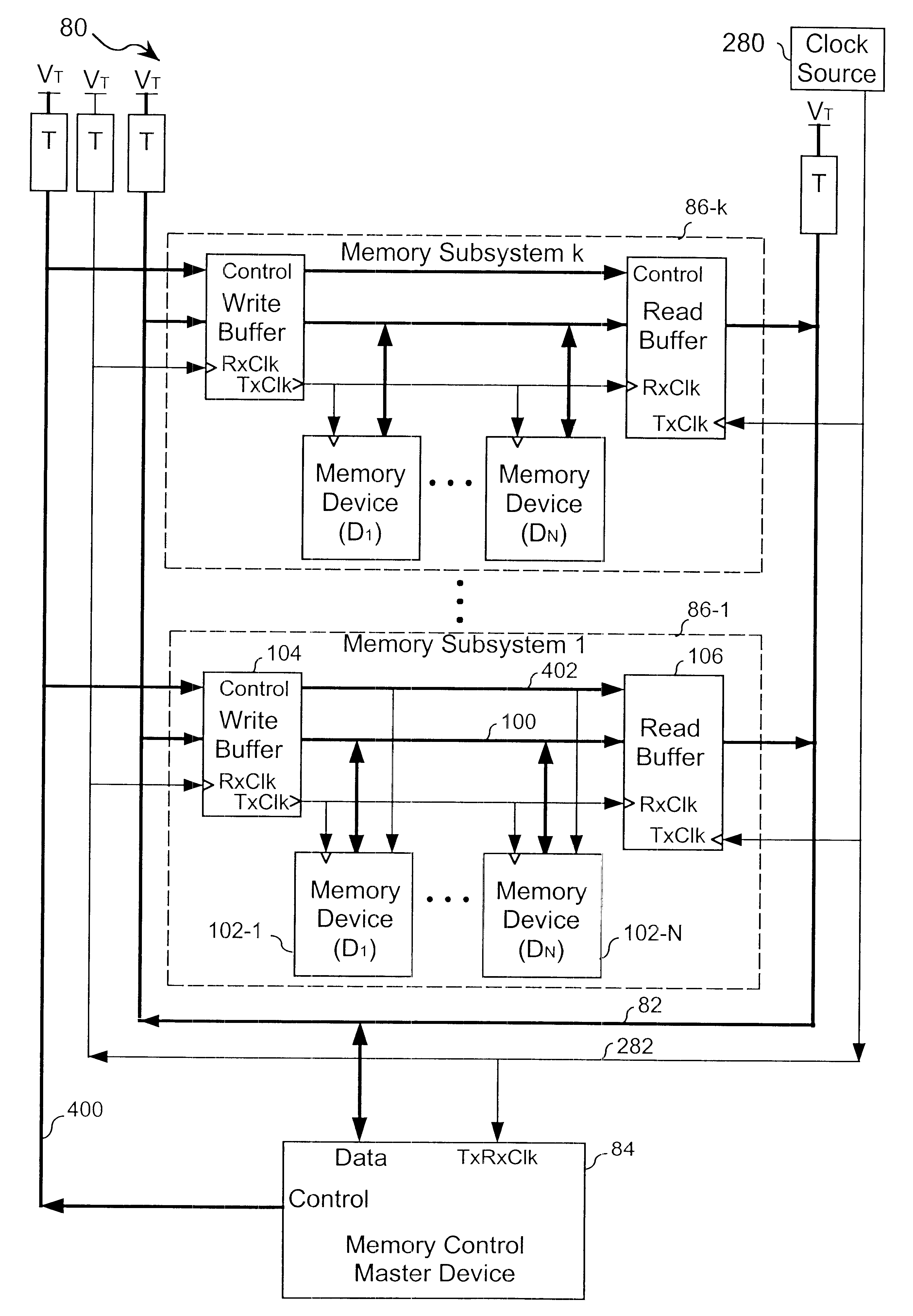
In FIG. 6, in a memory subsystem 120 for use in the memory system 80 of FIG. 5, a unidirectional local data bus 122 is terminated at first and second ends, 124 and 126, by first and second passive terminators 128 and 130, respectively. The local data bus 122 interconnects one or more memory devices 102, the write buffer 104 and the read buffer 106, as described above with respect to FIG. 5. For simplicity, a single local bus signal line 122 is shown. The local bus 122 has a first end 124 and a second end 126. In this memory subsystem configuration 120, the local bus signal line 122 is terminated at both ends by passive terminators 128 and 130. To use the same memory devices 42 as in the prior art memory system 50 of FIG. 1, the impedance of the signal line 122 is designed to equal twice the value of the loaded impedance Z.sub.L, used in the prior art memory system 50 (FIG. 1). Therefore, the terminators 128 and 130 have an impedance substantially equal to twice the loaded impedance ...
second embodiment
an Active Terminator
FIG. 8B shows a second implementation of an active terminator 170 with reduced complexity. The active terminator 170 has a PMOS transistor 172. The PMOS transistor 172 is sized such that its large-signal output resistance is equal to the loaded impedance Z.sub.L at the center of its voltage swing. In one implementation, the PMOS transistor 172 is sized to have a 28 ohm large signal output resistance when the voltage at the I / O pin is pulled down to 1.4V. Although the active terminator 170 provides an output resistance that is less linear that of the active terminator 160 (FIG. 8A), simulations indicated that the active terminator 170 is sufficiently linear to provide an acceptable termination. For example, in the simulation, the output resistance varied from 17 to 45 ohms over the range of voltage swing V.sub.Swing. The parasitic capacitance of the active terminator 170 did not significantly affect the termination impedance and, therefore, impede the proper opera...
third embodiment
a Memory Sub-system
FIG. 9 shows yet another embodiment of a memory subsystem 200 for use in the memory system 80 of FIG. 5. Like memory subsystem 140 of FIG. 7, the local bus signal line 202 in this memory subsystem 200 is terminated using both an active terminator 204 and a passive terminator 206. Although the local bus 202 has many local bus signal lines, for simplicity, a single local bus signal line 202 will be described. The local bus signal line 202 is terminated in a write buffer 210 with the active terminator 204 and is terminated at the read buffer 212 with the passive terminator 206. In this embodiment 200, the loaded impedance, Z.sub.L, of the local bus signal line 202 is the same as that of the prior art memory system 50 (FIG. 1) and both the active terminator 204 (when active) and the passive terminator 206 match the loaded impedance, Z.sub.L.
When writing data to a memory device, the write buffer 210 transmits data onto the local bus signal line 202 With the active term...
PUM
 Abstract
Description
Claims
Application Information


