

Power fail saving modes in solid state drive with mlc memory
a technology of solid state drives and fail saving modes, which is applied in the direction of static storage, digital storage, instruments, etc., can solve the problems of limited capacity, affecting the integrity of future data written to the device, and data in incomplete flash blocks may suffer corruption and errors, so as to prevent corruption of data pages and reduce holdup time
- Summary
- Abstract
- Description
- Claims
- Application Information
AI Technical Summary
Benefits of technology
Problems solved by technology
Method used
Image

Examples
Embodiment Construction
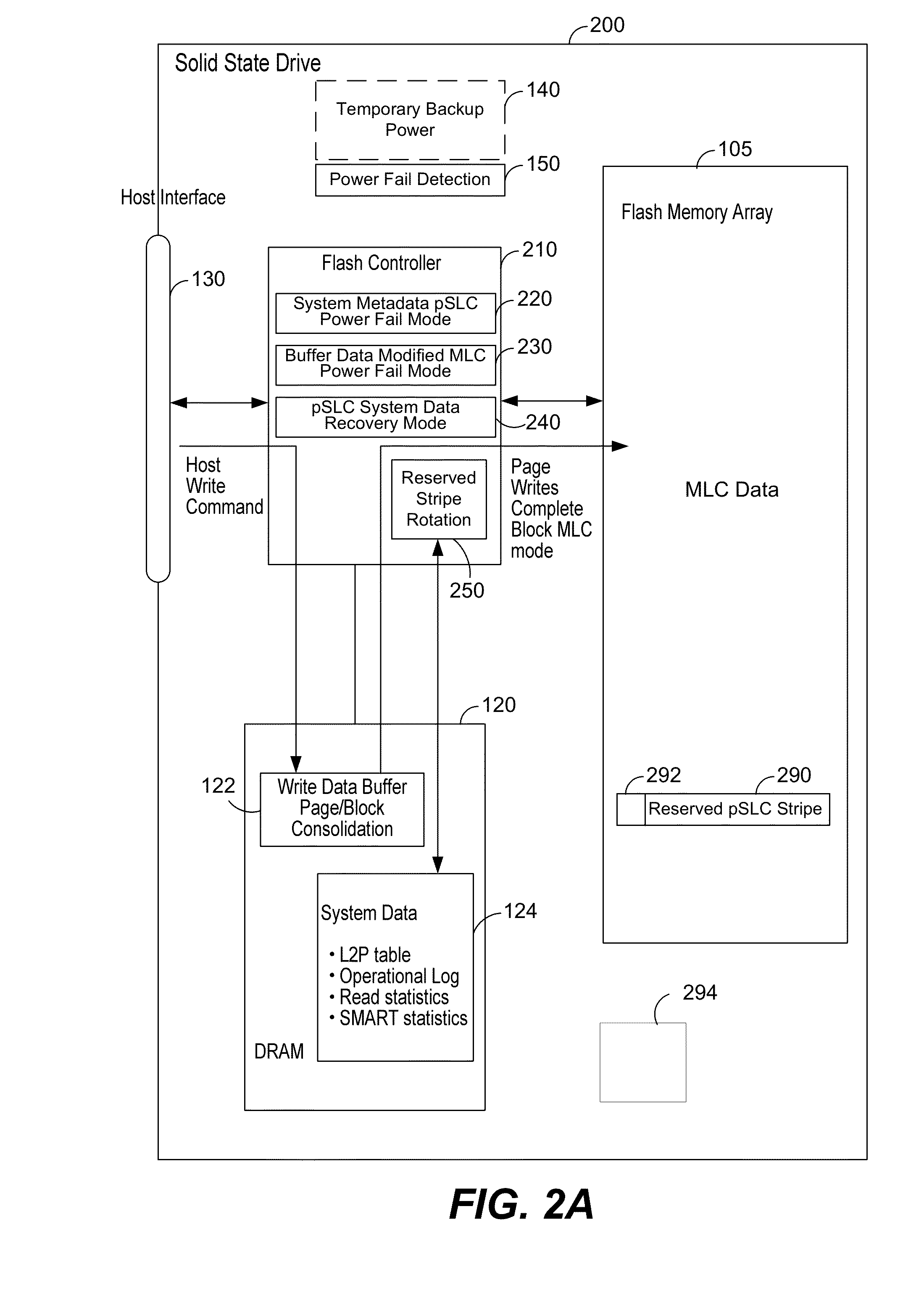
[0029]FIG. 2A is a schematic of a Solid State Drive (SSD) 200 operating in a normal multi-level cell (MLC) mode. The SSD 200 includes a flash memory array 105, a flash controller 210, and a dynamic random access memory (DRAM) 120. The DRAM 120 may be used to buffer user data with both read and write commands from the host to the flash memory controller 210. It may also be used to store system data such as L2P (Logical to Physical) address tables, an operational log (where the sequence of events processed by the controller can be saved for later inspection) and statistics concerning the read and write activity and SMART (Self-Monitoring, Analysis and Reporting Technology) data logging. This system data is commonly referred to as ‘metadata’ collectively.
[0030]For read commands, a portion of the DRAM 120 may be assigned to act as a read cache, where frequently accessed user data may be stored in the cache after reading from the memory array, and then subsequent reads for the same user ...
PUM
 Abstract
Description
Claims
Application Information