
Functional block for integrated circuit, semiconductor integrated circuit, inspection method for semiconductor integrated circuit, and designing method therefor

a technology of integrated circuits and functional blocks, which is applied in the direction of detecting faulty computer hardware, faulty hardware testing methods, instruments, etc., can solve the problems propagating and extremely complicated and difficult to produce test data patterns that should be propagated through the respective functional blocks. , to achieve the effect of reducing the number of steps of generating test data, and reducing the number of steps

Inactive Publication Date: 2004-03-16
PANASONIC CORP
View PDF9 Cites 13 Cited by
  • Summary
  • Abstract
  • Description
  • Claims
  • Application Information

AI Technical Summary

Benefits of technology

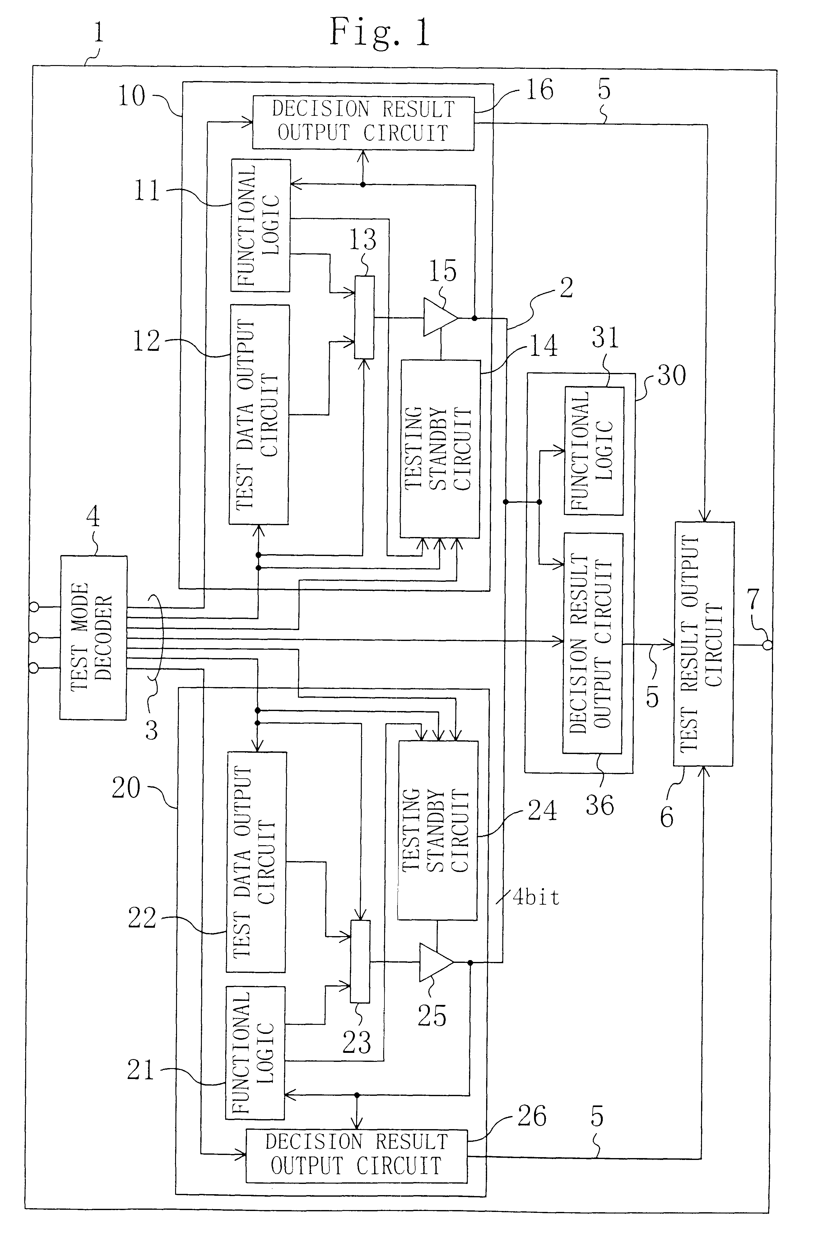
According to the first IC functional block, a test data output circuit for outputting test data is provided within the IC functional block. Thus, if a semiconductor integrated circuit is constructed of the block and another IC functional block including a circuit that can receive the test data and compare it to an expected value, then the test data can be transmitted and received even when the user does not know much about the internal configuration and operation of the IC functional blocks. Accordingly, even if IC functional blocks are combined or the circuit sizes of the IC functional blocks are huge, a test among the IC functional blocks can be carried out easily and accurately in the semiconductor integrated circuit.
As can be understood, even if the user does not know much about the configurations (i.e., the circuit or functional configurations) of the respective functional blocks 10, 20 and 30 or if the circuit sizes are too huge to produce test data with ease, the inter-block signal line 2 can be tested easily and accurately according to this embodiment.

Problems solved by technology

If a semiconductor integrated circuit is designed by combining a plurality of functional blocks with each other, however, there arises a problem in how to test a signal line interconnecting these functional blocks together.
However, if the first and second functional blocks 501 and 502 are combined and reused, it might be difficult for the user to produce test data patterns that should be propagated through the respective functional blocks.
This is because the user is not acquainted with the internal configurations and operations of the functional blocks.
Also, if the circuit sizes of the first and second functional blocks 501 and 502 are huge, then it is extremely complicated and very difficult to produce test data patterns that should be propagated through the respective functional blocks.
Thus, a large number of clock cycles should be consumed for that purpose, and it is difficult to supply the test data patterns rapidly and continuously enough to detect a fault promptly.

Method used


Image

  • Functional block for integrated circuit, semiconductor integrated circuit, inspection method for semiconductor integrated circuit, and designing method therefor
  • Functional block for integrated circuit, semiconductor integrated circuit, inspection method for semiconductor integrated circuit, and designing method therefor
  • Functional block for integrated circuit, semiconductor integrated circuit, inspection method for semiconductor integrated circuit, and designing method therefor

Examples


first embodiment

Hereinafter, a first modified example of the present invention will be described with reference to the drawings.

FIG. 6 illustrates circuit configurations of functional blocks and a semiconductor integrated circuit, which is made up of these functional blocks, according to a first modified example of the first embodiment. In FIG. 6, the same components as those illustrated in FIG. 1 are identified by the same reference numerals and the description thereof will be omitted herein. The semiconductor integrated circuit 1 shown in FIG. 6 includes first, second and third functional blocks 10, 20A and 30. This embodiment is characterized in that only one of the functional blocks 10, 20A and 30 included in the semiconductor integrated circuit 1 includes the test data output circuit. In the illustrated example, only the first functional block 10 includes the test data output circuit 12 as shown in FIG. 6.

In this configuration, the total circuit size of the functional blocks can be reduced com...

second modified example of first embodiment

Hereinafter, a second modified example of the first embodiment of the present invention will be described with reference to the drawings.

FIG. 7 illustrates circuit configurations of functional blocks and a semiconductor integrated circuit, which is made up of these functional blocks, according to a second modified example of the first embodiment. In FIG. 7, the same components as those illustrated in FIG. 6 are identified by the same reference numerals and the description thereof will be omitted herein. The semiconductor integrated circuit 1 shown in FIG. 7 includes first, second and third functional blocks 10A, 20A and 30. This embodiment is characterized in that only one of the functional blocks 10A, 20A and 30 included in the semiconductor integrated circuit 1 includes the test data output circuit. This embodiment is further characterized in that the first functional block 10A is a testing-dedicated functional block not including any circuit with a predetermined function that is ...

third modified example of first embodiment

Hereinafter, a third modified example of the first embodiment of the present invention will be described with reference to the drawings.

FIG. 8 illustrates circuit configurations of functional blocks and a semiconductor integrated circuit, which is made up of these functional blocks, according to a third modified example of the first embodiment. In FIG. 8, the same components as those illustrated in FIG. 7 are identified by the same reference numerals and the description thereof will be omitted herein. The semiconductor integrated circuit 1 shown in FIG. 8 includes first, second, third and fourth functional blocks 10A, 20B, 20C and 30A. Neither the second nor third functional block 20B, 20C includes any test data output circuit or decision result output circuit. Also, the fourth functional block 30A is a testing-dedicated functional block, which includes no circuit with a predetermined function, but consists of only the decision result output circuit 36.

In this configuration, the int...


PUM


Abstract

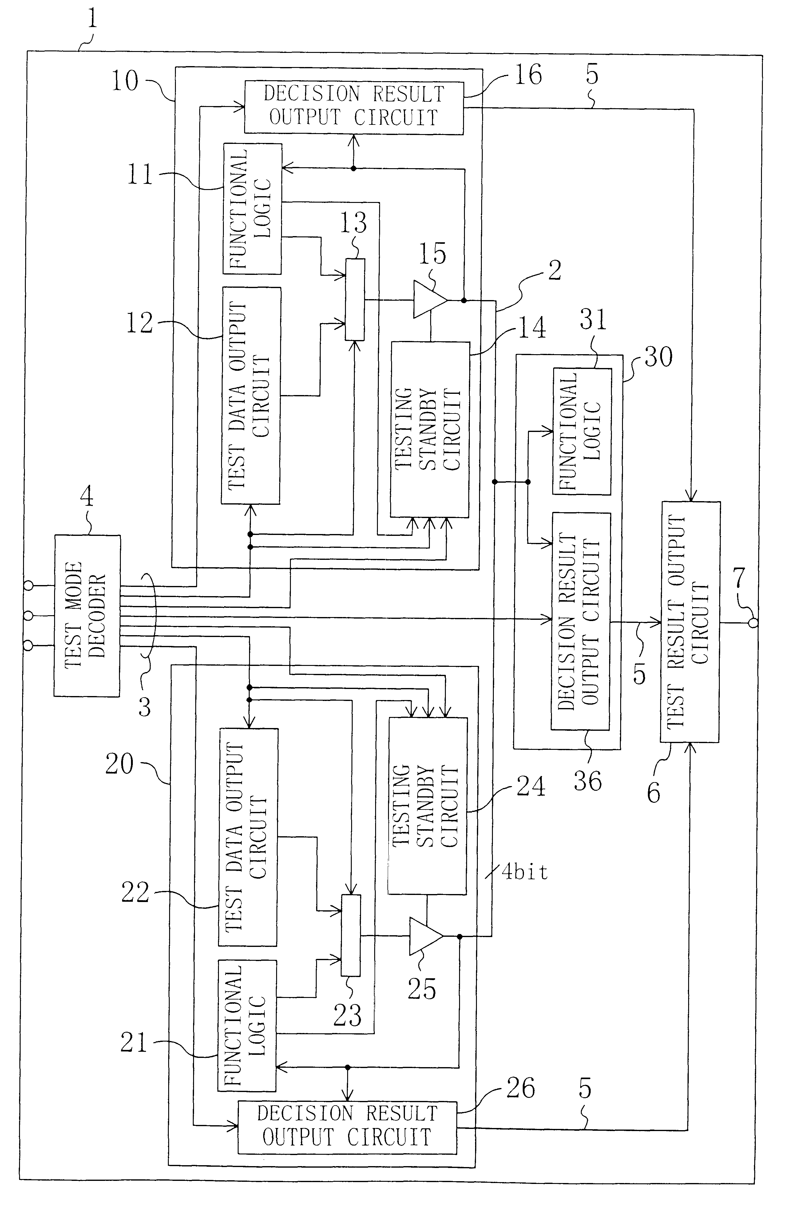
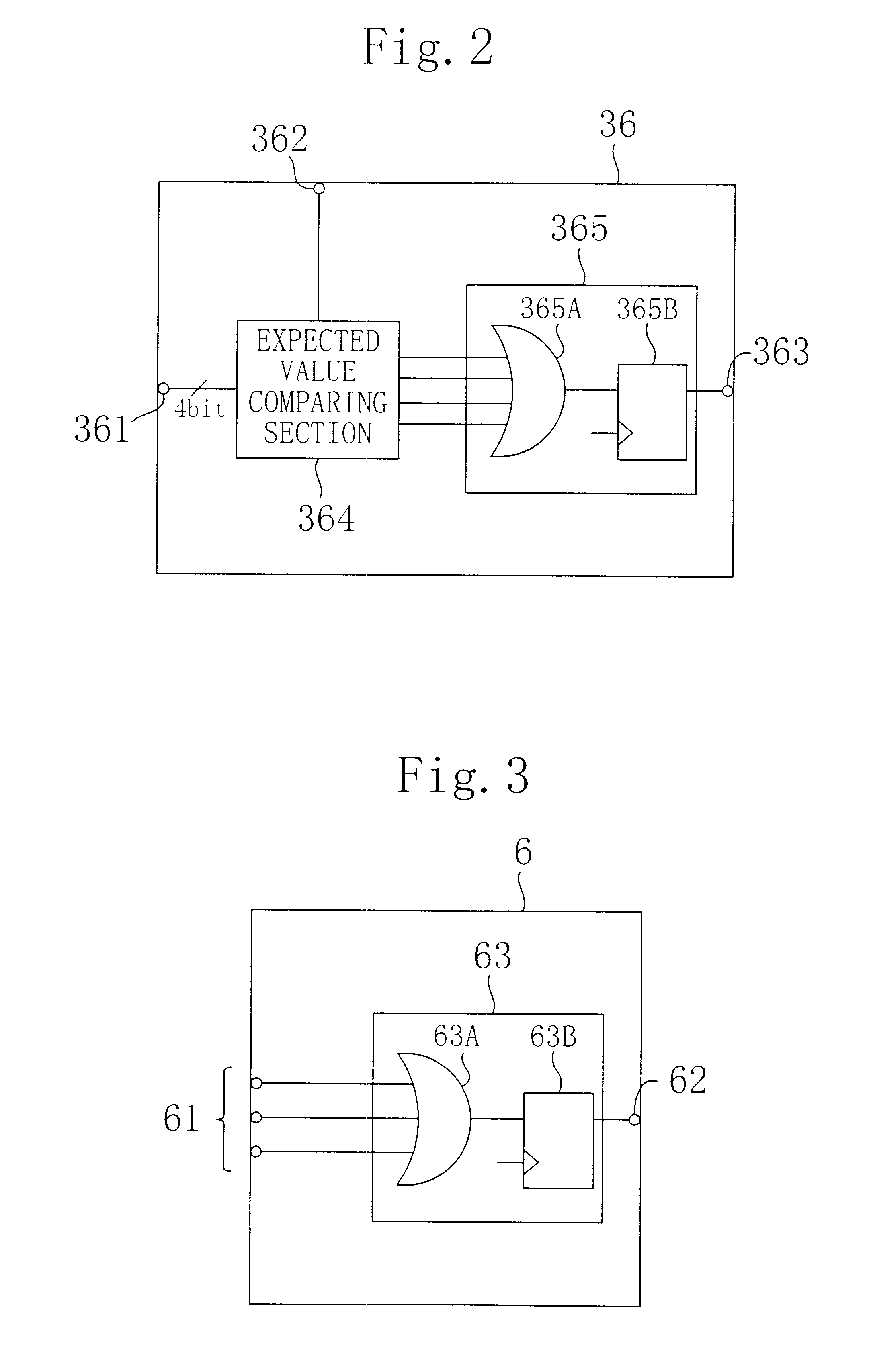
A semiconductor integrated circuit (1) includes first, second and second functional blocks (10, 20 and 30). The first, second and second functional blocks (10, 20 and 30) are coupled together via an inter-block signal line (2). The first functional block (10) includes: a logic circuit (11); a test data output circuit (12), which operates during testing and outputs a predetermined test data pattern; a testing standby circuit (14), which is connected between a selector (13) and an external bidirectional pin and makes the functional block enter a standby state during testing; a tristate buffer (15) that is made to have a high impedance by the testing standby circuit (14); and a decision result output circuit (16), which receives the test data pattern from the second functional block, compares the received test data pattern to an expected value stored therein, and outputs a decision result to a decision result signal line (5).

Description

The present invention relates to a functional block for integrated circuit (hereinafter, simply referred to as an "IC functional block") implemented as a macro cell including a self-diagnosis circuit for detecting a fault between functional blocks, for example. The present invention also relates to a semiconductor integrated circuit that has been designed using the IC functional block and to respective methods for testing and designing the semiconductor integrated circuit.In recent years, demand for designing a semiconductor integrated circuit more efficiently by implementing the circuit as a combination of functional blocks such as macro cells has been increasing. If a semiconductor integrated circuit is designed by combining a plurality of functional blocks with each other, however, there arises a problem in how to test a signal line interconnecting these functional blocks together. To solve this problem, according to a conventional technique, the operations of a pair of functiona...

Claims


Application Information

Patent Timeline
IPC IPC(8): H01L27/02G06F11/22
CPCH01L27/0207G06F11/2273H01L27/04
Inventor OHTA, MITSUYASUTAKEOKA, SADAMIHIRAOKA, TOSHIHIRO
Owner PANASONIC CORP
Learn More