Thin film transistor and display device having the same

a thin film transistor and display device technology, applied in the field of transparent thin film transistors and display devices having the same, can solve the problems of lowering the light transmittance, complicating the steps, and unable to adapt the structure in which light is transmitted through the tft portion,

Inactive Publication Date: 2004-03-30
FUJIFILM BUSINESS INNOVATION CORP
View PDF4 Cites 27 Cited by
  • Summary
  • Abstract
  • Description
  • Claims
  • Application Information

AI Technical Summary

Problems solved by technology

In this case, since amorphous silicon forming the transistor is photo-conductive, it is necessary to shield light so that the light from the back light for the display of liquid crystals is not incident to amorphous silicon for accurate operation only by the voltage, as well as light shielding is necessary for preventing erroneous operation also in a case of utilizing light incidence from the outside as in a reflection type since amorphous silicon is sensitive to visible light, which, however, results in a problem of complicating the steps.
Further, since amorphous silicon has absorption for visible light, it is impossible to adapt a structure in which light is transmitted through the TFT portion.
However, when the size of the pixel is reduced, an area ratio (open ratio) between a pixel-forming TFT portion not transmitting light and a pixel electrode capable of transmitting light and driving liquid crystals is decreased to result in a problem of lowering the light transmittance and darkening the display, and also increasing electric power consumption.
Further, since the pixel itself depends on the area of the pixel electrode excluding the opaque TFT, it results in a problem of reducing the size of the pixel.
Further, although a structure of using a glass substrate has also been proposed (J. Cryst, Growth 189 / 190 (1998) 749 to 752), since it uses the source-drain electrodes of an Al film and the Al gate electrode, and it cannot be used for a transparent device.

Method used


Image

  • Thin film transistor and display device having the same
  • Thin film transistor and display device having the same
  • Thin film transistor and display device having the same

Examples


first embodiment

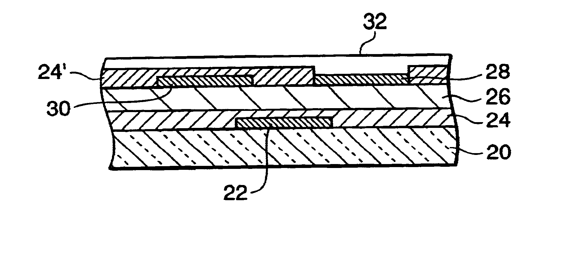
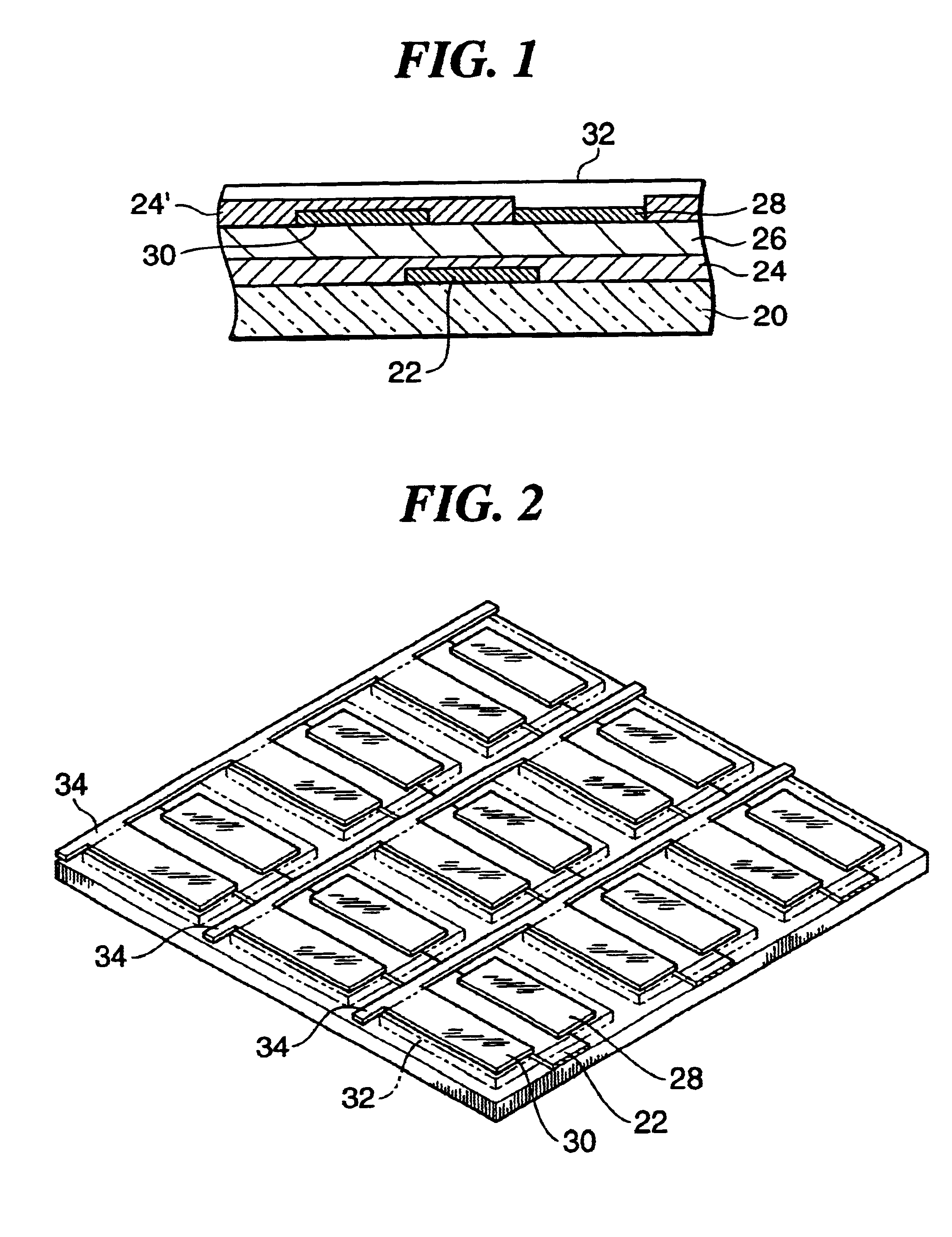
FIG. 1 is a schematic cross-sectional view of a thin film transistor as a first embodiment according to this invention. The thin film transistor of the first embodiment is an inverted stagger type thin film transistor having a constitution including, as shown in FIG. 1, a transparent substrate 20, a transparent gate electrode 22 disposed on the transparent substrate 20, a transparent insulative layer 24 disposed so as to cover the transparent gate electrode 22, a transparent semiconductor layer 26 disposed on the transparent insulative layer 24, a transparent source electrode 28 and a transparent drain electrode 30 disposed on the transparent semiconductor layer 26, a transparent insulative layer 24' disposed so as to cover the transparent drain electrode 30, a transparent pixel electrode 32 covering the transparent insulative layer 24' and in connection with the transparent source electrode 28.

In the thin film transistor of the first embodiment, as shown in FIG. 2, the transparent ...

second embodiment

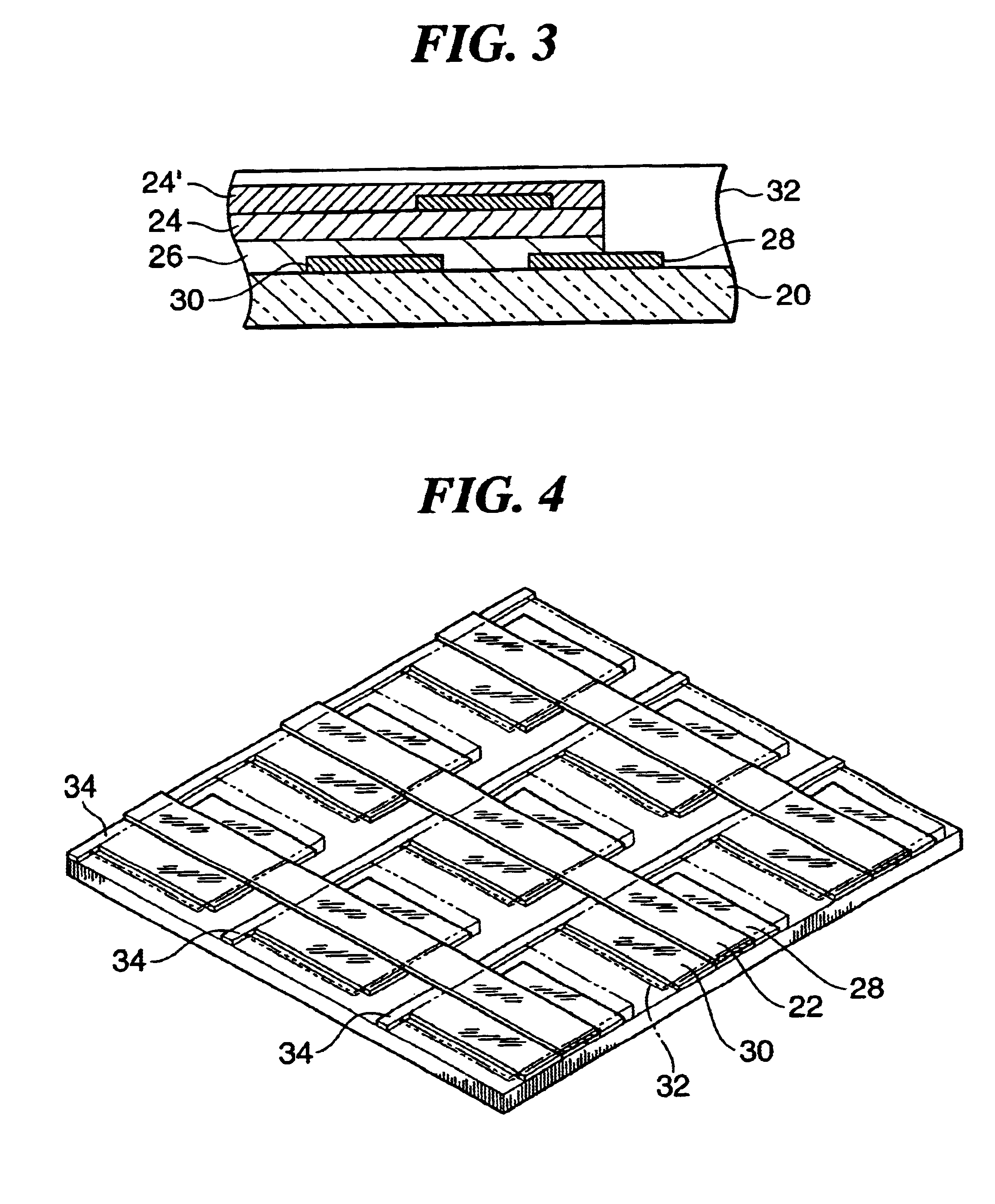
FIG. 3 is a schematic cross-sectional view of a thin film transistor as a second embodiment according to this invention. The thin film transistor of the second embodiment is a stagger type thin film transistor having a constitution including a transparent substrate 20, a transparent source electrode 28 and a transparent drain electrode 30 disposed on the transparent substrate 20, a transparent semiconductor layer 26 disposed so as to cover the transparent drain electrode 30 entirely and the transparent source electrode 28 partially, a transparent insulative layer 24 disposed on the transparent semiconductor layer 26, a transparent gate electrode 22 disposed on the transparent insulative layer 24, a transparent insulative layer 24' so as to cover the transparent gate electrode 22, and a transparent pixel electrode 32 so as to cover the transparent insulative layer 24' and in contact with the transparent source electrode 28.

As shown in FIG. 4, in the thin film transistor of second emb...

example 1

ITO was formed as film of 2 mm both in width and length and 200 nm in thickness by sputtering on cleaned Corning 7059 to form a transparent gate electrode. Insulative amorphous AlGaN:H was formed to a film of 200 nm in thickness so as to cover the gate electrode while leaving one end to form a transparent insulative film. An undoped GaN:H film was formed on the transparent insulative layer to form a transparent semiconductor layer. ITO was formed as two films each of 200 .mu.m both in width and length and 100 nm in thickness at a gap distance of 50 .mu.m (by two) on the transparent substrate layer to form a transparent source electrode and a transparent drain electrode. Thus a transparent device was manufactured.

When a voltage at 5 V was applied between the transparent source electrode and the transparent drain electrode in this device, 0.5 to 1 .mu.A of a current was obtained at gate voltage of 10 V on the gate electrode, and it could be confirmed that the device operated as a tran...


PUM

PropertyMeasurementUnit
transmittanceaaaaaaaaaa
thicknessaaaaaaaaaa
sizeaaaaaaaaaa

Abstract

A thin film transistor has, on a transparent substrate, a transparent semiconductor layer containing nitrogen, hydrogen and one or more elements selected from Al, Ga and In, a transparent source electrode and a transparent drain electrode at least partially in contact with the transparent semiconductor layer, and a transparent gate electrode.

Description

1. Field of the InventionThis invention relates to a transparent thin film transistor and a display device having the same and, for example, it relates to a thin film transistor capable of coping with higher image quality and higher definition of a display device, as well as a display device using the thin film transistor described above.2. Description of the Related ArtHigher image quality and higher definition for display devices have been developed rapidly in recent years and there has been a demand for reduction of the size of pixels. Usually in display devices using liquid crystals, a system of using thin film transistors (TFT) and driving them on every pixel has been adopted. For the operation, TFT using amorphous silicon is usually used, and liquid crystals driven by transparent pixel electrodes connected with transistors can be seen through back light. In this case, since amorphous silicon forming the transistor is photo-conductive, it is necessary to shield light so that th...

Claims


Application Information

Patent Timeline
Patent Type & Authority Patents(United States)
IPC IPC(8): H01L21/02H01L21/336H01L29/40H01L29/66H01L27/12H01L29/45H01L29/49H01L29/786G02F1/13G02F1/1368
CPCH01L27/12H01L29/458H01L29/4908H01L29/66742H01L29/78603H01L29/78681G02F1/1368
Inventor YAGI, SHIGERU
Owner FUJIFILM BUSINESS INNOVATION CORP
Why Eureka
Try Eureka