

Magnetic random access memory
a random access and magnetic technology, applied in the field of magnetic random access memory, can solve problems such as difficulty in enlarge the memory capacity
- Summary
- Abstract
- Description
- Claims
- Application Information
AI Technical Summary
Benefits of technology
Problems solved by technology
Method used
Image

Examples
example 2
(2) Structure Example 2
Structure Example 2 is different from Structure Example 1 in that the direction of the read select switch (MOS transistor) RSWL disposed in the read block is rotated by 90.degree..
In the Structure Example 2, since the channel width of the read select switch RSW1 is equal to the width of the Y-direction, the channel width of the read select switch RSW1 is easily enlarged. That is, in Structure Example 2, the channel width of the read select switch RSW1 is enlarged, the read current is increased, and the read operation can be stabilized.
(2)-1 Circuit Structure
The circuit structure will first be described.
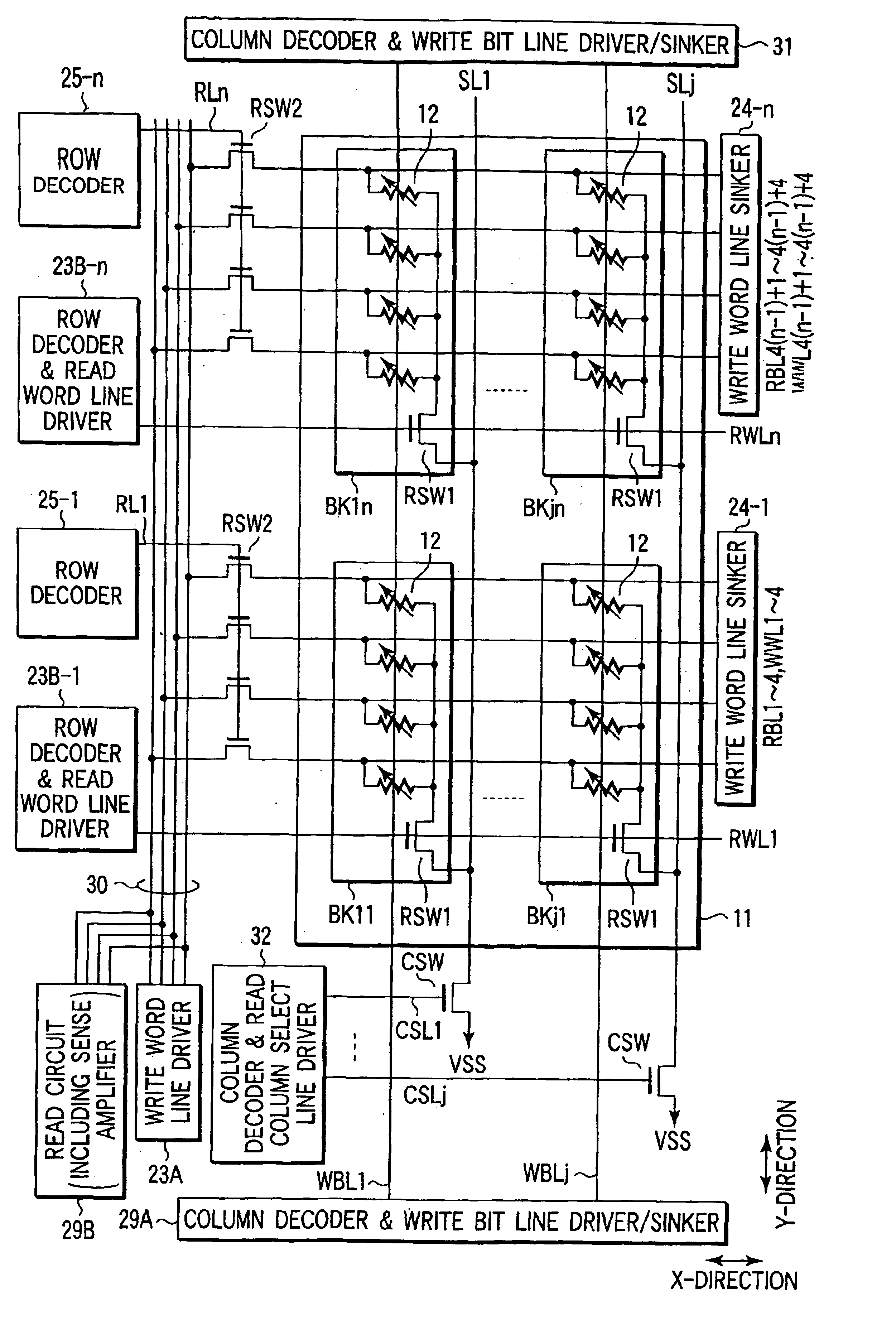
FIG. 14 shows the main part of the magnetic random access memory as Structure Example 2 of the present invention.
The memory cell array 11 has a plurality of TMR elements 12 arranged in an array in the X and Y-directions. In the X-direction, the j TMR elements 12 are arranged, and in the Y-direction, 4.times.n TMR elements 12 are arranged.
Four TMR elements 12 arr...
example 3
(3) Structure Example 3
Structure Example 3 is a modification example of Structure Example 1 in that the axis of easy magnetization of the TMR element of Structure Example 1is rotated by 90.degree..
In Structure Examples 1, 2, each axis of easy magnetization of each TMR element turns to the X-direction, and an axis of difficult magnetization turns to the Y-direction (column direction). That is, the TMR element has the rectangular shape elongated in the X-direction. On the other hand, in Structure Example 3, the axis of easy magnetization of the TMR element turns to the Y-direction, and the axis of difficult magnetization turns to the X-direction. That is, Structure Example 3 has a characteristic that the TMR element has the rectangular shape elongated in the Y-direction.
With the magnetic random access memory, the direction of the write current flowing through a write line extending in a direction parallel to the axis of difficult magnetization, and the data is written in the memory ce...
example 4
(4)-1 Structure Example 4
FIG. 26 shows the main part of the magnetic random access memory as Structure Example 4 of the present invention.
Structure Example 4 is characterized in that a bias potential VC is given to one end of each of four TMR elements 12 constituting the read block BKik.
That is, in Structure Example 1 (FIG. 1), the source line SLi is connected to the ground point VSS via the column select switch CSW. Therefore, in Structure Example 1, during the read operation, the read circuit 29B generates the bias potential VC, and the read current is supplied to the TMR element 12 from the read circuit 29B.
On the other hand, in Structure Example 4, the source line SLi connected in common to one end of each of four TMR elements 12 constituting the read block BKik is connected to a bias line 34 via the column select switch CSW.
Therefore, during the read operation, the bias potential VC is given to the bias line 34, and the read current is given to the TMR element 12 via the bias l...
PUM
 Abstract
Description
Claims
Application Information