
Shadow moire surface measurement using Talbot effect

a shadow moire and surface measurement technology, applied in the field of surface measurement, can solve the problems of increasing the time required for inspection of wafers during production, introducing distortion, and current techniques may distort the wafer, so as to and improve the accuracy of measurement.

Inactive Publication Date: 2004-05-04
THE RES FOUND OF STATE UNIV OF NEW YORK
View PDF5 Cites 105 Cited by
  • Summary
  • Abstract
  • Description
  • Claims
  • Application Information

AI Technical Summary

Benefits of technology

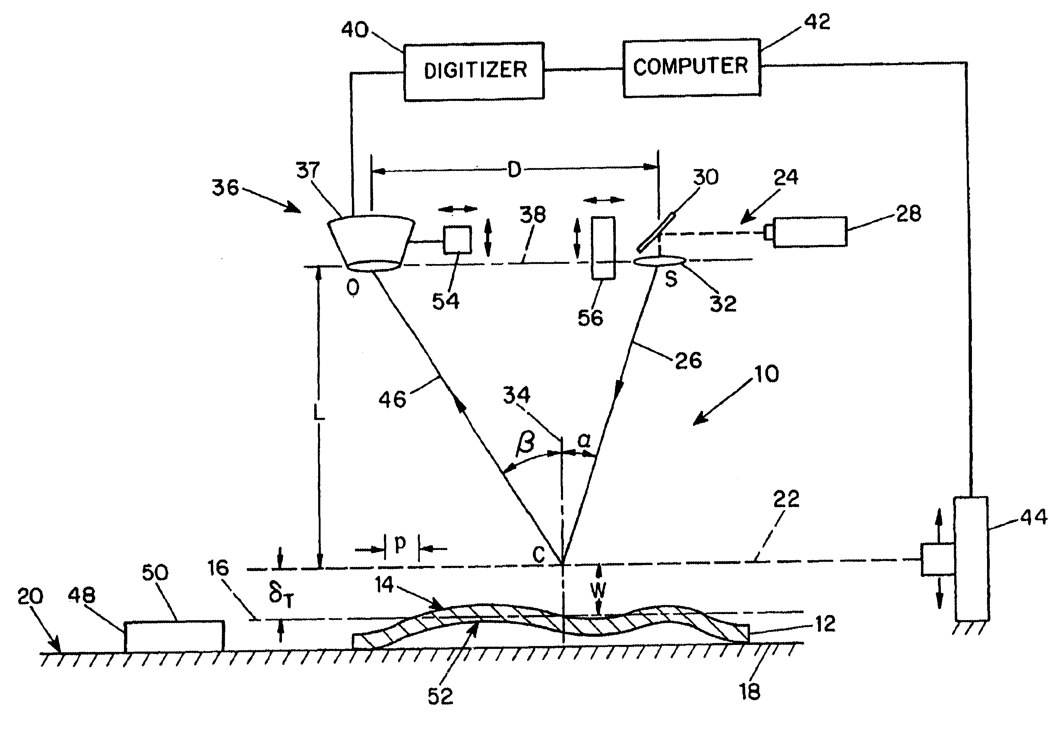
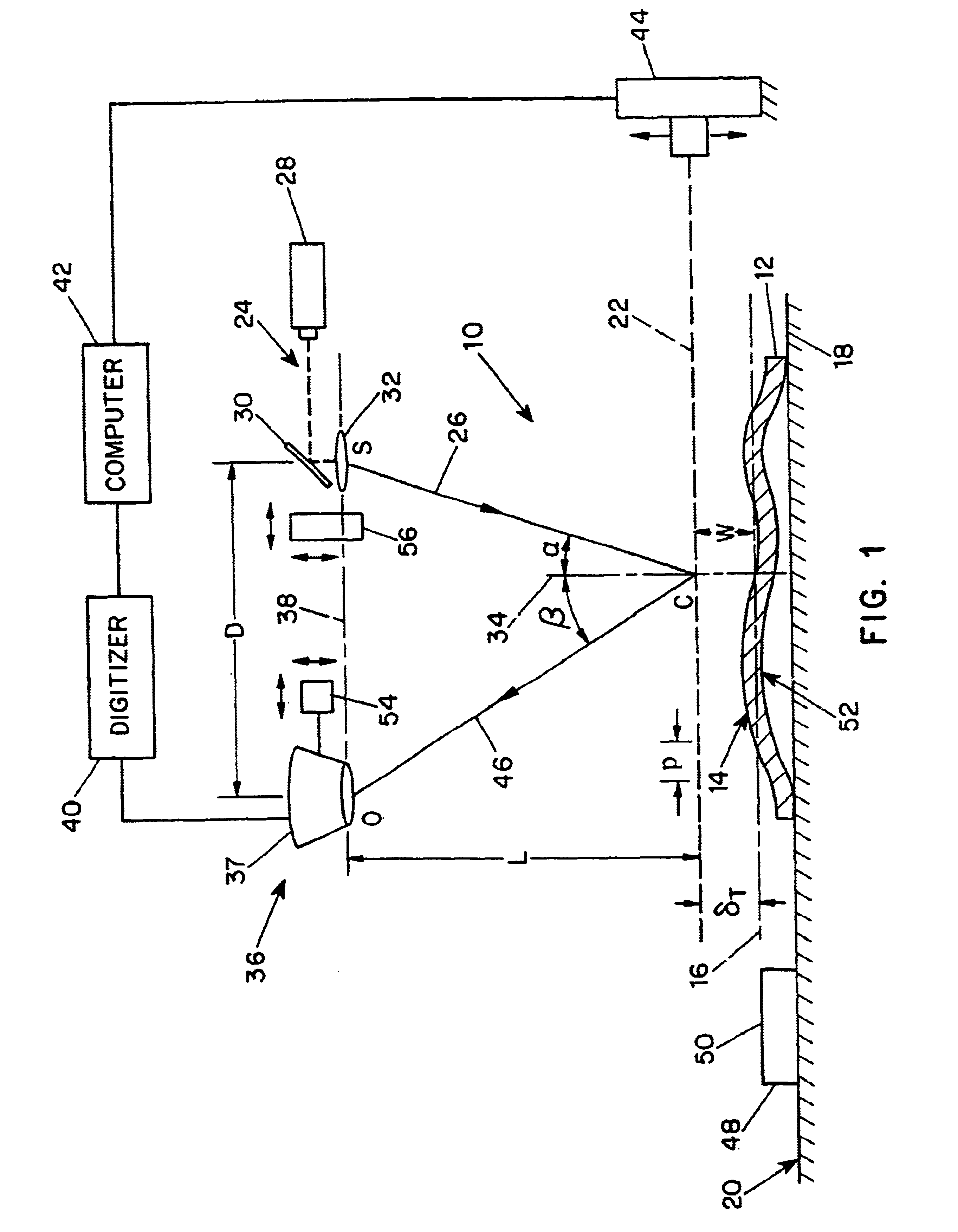
As noted above, one advantage of the present invention is the fact that the entire specimen surface 14 or 52 can be measured substantially simultaneously. Thus, with reference to FIGS. 1 and 7, it should be appreciated that first beam of light 26, although shown for illustrative convenience as a single line, can normally be formed so that it illuminates substantially all of the surface to be measured 14. Similarly, detector 36, such as camera 37, can be positioned to detect the moire fringes for substantially all of the surface to be measured 14 substantially simultaneously. Again, return light beam 46, although shown in FIGS. 1 and 7 as a line, would normally have sufficient diameter to encompass the entire surface to be measured 14 of the specimen 12.

Problems solved by technology

There are a number of disadvantages associated with the current method.
In order to obtain accurate measurements, numerous sampling points on the surface are needed, thus increasing the time required for inspection of wafers during production.
Further, current techniques may distort the wafer which is being measured during the measurement process.
Such distortions are introduced by the stress applied by the vacuum gripper, and also due to dynamic stresses caused by the high angular velocities used when spinning the wafer in order to traverse the capacitive probes.
However, there is always the potential for misalignment, i.e., a minute angle between reference grating 22 and specimen plane 20.
However, when p becomes very small (for example, a spatial frequency of about 1000 lines / inch or larger), the diffraction of light passing through the gratings becomes more significant, resulting in unclear fringes.
With such a fine pitch for the reference grating 22, diffraction effects become problematic, and as a result, the fringe patterns may be blurred.
However, there are limits to such increase as this may cause the size of the equipment to become too large to be practical.
Prior capacitive probe devices have normally been limited to round wafers.
A 1000 line per inch grating might be good for viewing the curves, but would not have enough resolution to detect roughness in the flat part.

Method used


Image

  • Shadow moire surface measurement using Talbot effect
  • Shadow moire surface measurement using Talbot effect
  • Shadow moire surface measurement using Talbot effect

Examples


example 2

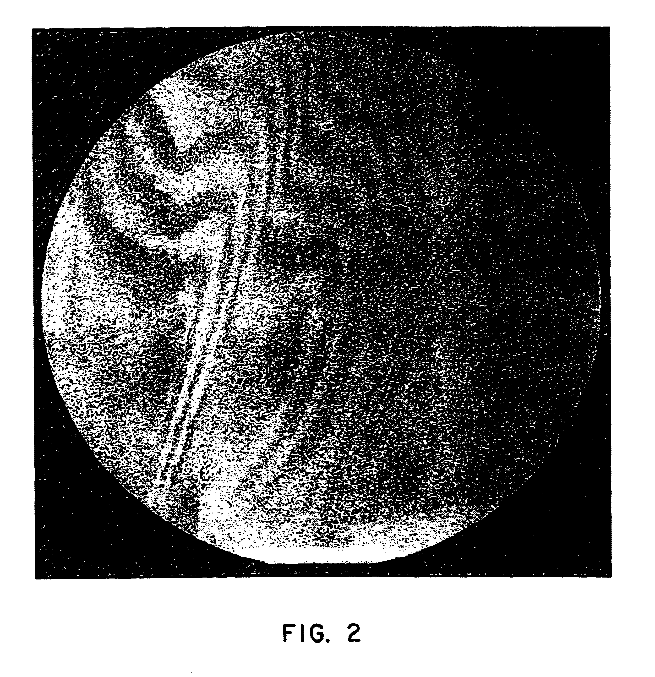
Experimental measurements were conducted on a 100 by 90 millimeter polycrystalline substrate wafer as shown in FIG. 3. The test setup and parameters were otherwise identical to that for FIG. 2. The wafer for this example was sliced by an HCT wiresaw. During the slicing process, change of wire took place due to wire rupture. As a result, there was a visible pause line on the wafer surface, about 25 millimeters from the left edge. The moire fringes in FIG. 3 successfully capture the pause caused by the manufacturing process. The three dimensional surface topography is shown in FIG. 6, obtained by the same process of digitizing as for the wafer in Example 1. From the fringe pattern in FIG. 3 and the three dimensional topography in FIG. 6, it is found that the surface jump occurs at x.congruent.25 millimeters with a depth jump of .DELTA.w .congruent.17 microns, which corresponds to the difference of one fringe order. By measuring the actual wafer, the change in depth was found at x=25 m...

example 3

Preliminary investigations have been performed with a 5000 line per inch grating. Visual observation has been carried out, but no images have been prepared. While diffraction makes it more difficult to capture images, basic patterns are discernible.


PUM


Abstract

A method and apparatus for surface measurement using the shadow moire effect with the Talbot effect. The apparatus includes a specimen mount to receive a specimen having a surface to be measured, and a reference grating mounted adjacent to the specimen mount so as to be substantially parallel to a mean surface plane of the specimen. The reference grating is mounted in such a manner that the distance between the reference grating and the mean surface plane of the specimen can be adjusted to a Talbot distance deltaT. The apparatus also includes a light source to illuminate the specimen through the grating and a detector positioned to detect the moire fringes produced by the grating due to variation of the surface of the specimen.

Description

BACKGROUND OF INVENTION1. Field of the InventionThe present invention relates to surface measurement, and more particularly relates to surface measurement using a shadow moire technique with the Talbot effect.2. Brief Description of the Prior ArtSurface measurement is required in the field of electronic device fabrication including, for example, fabrication of semiconductor devices. At the present time, wafers for fabricating such devices are slice either by an inner diameter saw or a wiresaw, followed by a series of lapping and polishing processes. A measuring device is necessary for measuring the flatness of the surface of the wafers after each manufacturing step. At the present time, such measurements are typically performed using a pair of capacitive probes to sample points on the surface of a rotating wafer.In the method currently practiced, wafers are handled with a vacuum gripper to hold the wafer at the center and to spin it at high speed while the traversing capacitive prob...

Claims


Application Information

Patent Timeline
Patent Type & Authority Patents(United States)
IPC IPC(8): G01B11/24G01B11/25
CPCG01B11/254
Inventor KAO, IMINCHIANG, FU-PEN
Owner THE RES FOUND OF STATE UNIV OF NEW YORK
Learn More