Method for fabricating an ultralow dielectric constant material

a dielectric constant and ultra-low technology, applied in the direction of chemical vapor deposition coating, semiconductor/solid-state device details, coatings, etc., can solve the problems of increasing signal delays in ulsi electronic devices, dielectric materials are not thermally stable, and dielectrics are rendered useless during integration

Inactive Publication Date: 2004-08-03
INTEL CORP
View PDF2 Cites 55 Cited by
  • Summary
  • Abstract
  • Description
  • Claims
  • Application Information

AI Technical Summary

Benefits of technology

It is a further object of the present invention to provide an improved method for fabricating an ultralow dielectric constant film in a parallel plate plasma enhanced chemical vapor deposition ("PECVD") reactor.
It is yet a further object of the present invention to provide an improved method for fabricating an ultralow dielectric constant material by depositing a film on a substrate in the presence of CO.sub.2 or CO.sub.2 and O.sub.2, thereby improving uniformity of the film deposited and stabilizing the plasma within the PECVD reactor.
It is yet another object of the present invention to provide a thermally stable ultralow dielectric constant material that has low internal stresses and a dielectric constant of not higher than about 2.8. More preferably, the dielectric constant for the ultralow-k material is in a range of about 1.5 to about 2.5 and, most preferably, the dielectric constant is in a range of about 2.0 to about 2.25.
In accordance with the present invention, there is provided an improved method for fabricating a thermally stable dielectric material that has a matrix comprising Si, C, O, and H atoms and an atomic level nanoporosity. In a preferred embodiment, the dielectric material has a matrix that consists essentially of Si, C, O, and H. The present invention further provides an improved method for fabricating the dielectric material by reacting a first precursor gas comprising atoms of Si, C, O, and H and at least a second precursor gas comprising atoms of C, H, and optionally O, F and N in a plasma enhanced chemical vapor deposition ("PECVD") reactor. The present invention yet further provides for mixing the first precursor gas with CO.sub.2, or mixing the first and second precursor gases with CO.sub.2 and O.sub.2, thereby stabilizing the plasma in the PECVD reactor and improving the uniformity of the film deposited on the substrate.

Problems solved by technology

This combined effect increases signal delays in ULSI electronic devices.
However, these dielectric materials are not thermally stable when exposed to temperatures above 300.about.350.degree. C.
Consequently, these dielectrics are rendered useless during integration.
Furthermore, the precursor materials are high cost and prohibitive for use in mass production.

Method used


Image

  • Method for fabricating an ultralow dielectric constant material
  • Method for fabricating an ultralow dielectric constant material
  • Method for fabricating an ultralow dielectric constant material

Examples


example 1

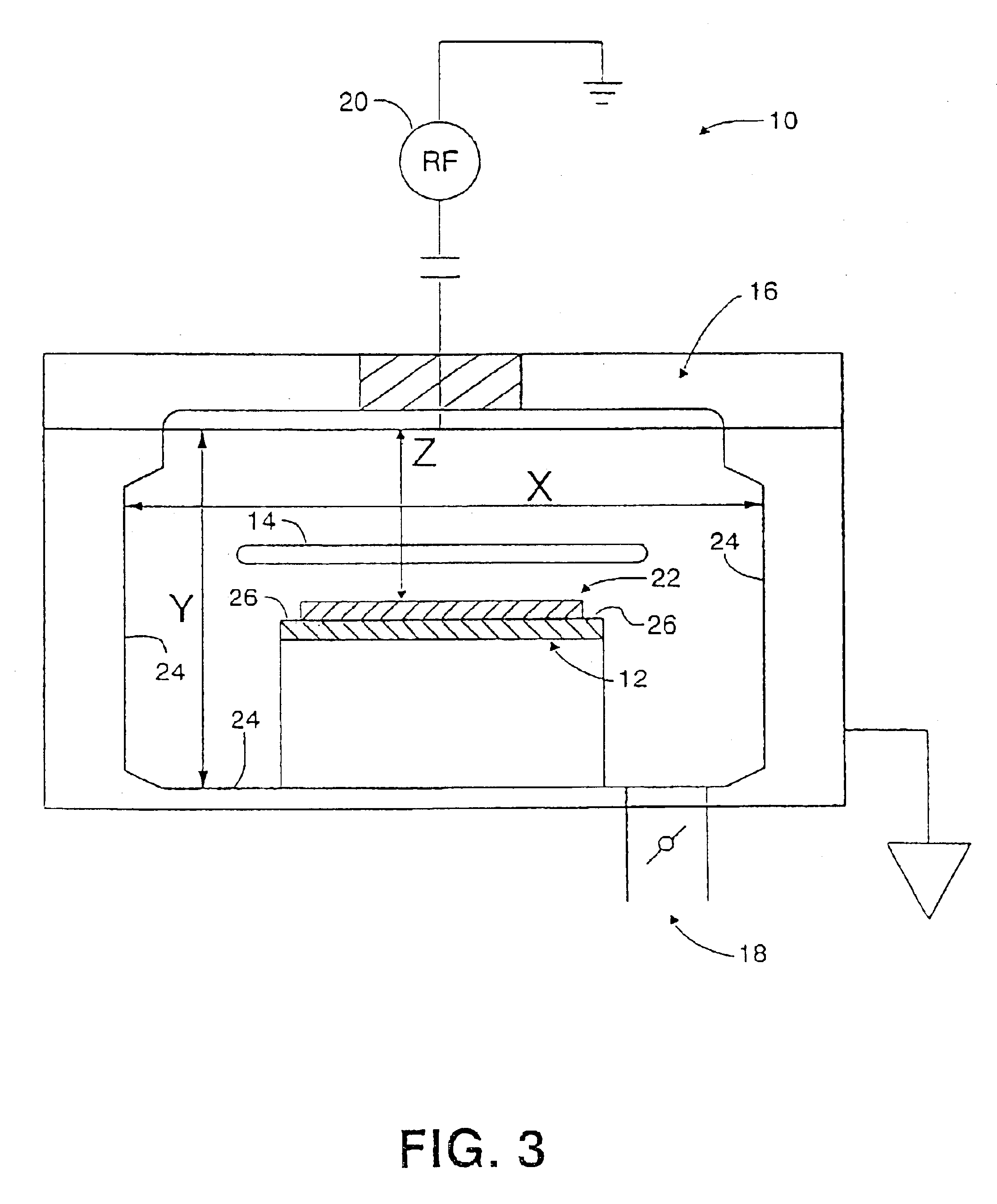
In this example, according to FIG. 3, a wafer is first prepared by introducing the wafer into reactor 10 through a slit valve 14 and pre-etching the wafer by argon gas. In this wafer preparation process, the wafer temperature is set at about 180.degree. C. and the argon flow rate is set at about 25 sccm, to achieve a pressure of about 100 mTorr. A RF power is then turned on to about 125 W for about 60 seconds. The RF power and the argon gas flow are then turned off.

The TMCTS precursor is carried into the reactor reactor using CO.sub.2 as a carrier gas; CO.sub.2 is at a pressure of about 5 psig at the inlet to the TMCTS container. The ultralow-k film according to the present invention can be deposited by first establishing gas flows of TMCTS+CO.sub.2 and CPO to desired flow rates and pressure, i.e., at about 20 sccm of TMCTS+CO.sub.2 and about 10 sccm of CPO and about 100 mTorr. A RF power is then turned on at about 15 W for a time period of about 50 minutes. The RF power and the gas...

example 2

In this example, a wafer is prepared as described in Example 1, but the wafer temperature is set at about 300.degree. C. The TMCTS precursor is then carried into the reactor using CO.sub.2 as a carrier gas; CO.sub.2 is at a pressure of about 5 psig at the inlet to the TMCTS container. The ultralow-k film according to the present invention can be deposited by first establishing gas flows of TMCTS+CO.sub.2 and CPO to desired flow rates and pressure, i.e., at about 150 sccm of TMCTS+CO.sub.2 and about 75 sccm of CPO and about 2000 mTorr. A RF power is then turned on at about 150 W for a time period of about 10 minutes. The RF power and the gas flow are then turned off. The wafer is then removed from the reaction reactor 10 and annealed as described in Example 1.

In the foregoing examples, the plasma was operated in a continuous mode. In Example 3 herein below, the plasma is operated in a pulsed mode.

example 3

In this example, the deposition is performed under conditions similar to Example 1, but the plasma is operated in a pulsed mode, i.e., with a duty cycle of about 50% and a plasma-on time of about 50 msec to about 100 msec. After removal of the wafer from reactor 10, the wafer with the deposited film is annealed as described in Example 1.


PUM

PropertyMeasurementUnit
temperatureaaaaaaaaaa
dielectric constantaaaaaaaaaa

Abstract

A method for fabricating a thermally stable ultralow dielectric constant film comprising Si, C, O and H atoms in a parallel plate chemical vapor deposition process utilizing plasma enhanced chemical vapor deposition ("PECVD") process is disclosed. To enable the fabrication of thermally stable ultralow dielectric constant film, specific precursor materials are used, such as, cyclic siloxanes and organic molecules containing ring structures, for instance, tetramethylcycloterasiloxane and cyclopentene oxide. To stabilize plasma in the PECVD reactor and thereby improve uniformity of the deposited film, CO2 is added to TMCTS as a carrier gas, or CO2 or a mixture of CO2 and O2 are added to the PECVD reactor.

Description

1. Technical Field of the InventionThe present invention generally relates to a method for fabricating a dielectric material that has an ultralow dielectric constant (or ultralow-k) associated therewith. More particularly, the present invention relates to an improved method for fabricating a thermally stable ultralow-k film for use as an intralevel or interlevel dielectric in an ultra-large-scale integration ("ULSI") back-end-of-the-line ("BEOL") wiring structure.2. Description of the Prior ArtThe continuous shrinking in dimensions of electronic devices utilized in ULSI circuits in recent years has resulted in increasing the resistance of the BEOL metallization as well as increasing the capacitance of the intralayer and interlayer dielectric. This combined effect increases signal delays in ULSI electronic devices. In order to improve the switching performance of future ULSI circuits, low dielectric constant (k) insulators and particularly those with k significantly lower than silico...

Claims


Application Information

Patent Timeline
Patent Type & Authority Patents(United States)
IPC IPC(8): C23C16/40H01L21/02H01L23/532H01L21/316H01L23/52H01L21/312H01L21/768H01L23/522
CPCC23C16/401H01L21/02126H01L21/02216H01L21/02274H01L21/3122H01L21/31633H01L23/5329H01L23/53295H01L2924/0002H01L2924/00B82Y40/00H01L21/20
Inventor GRILL, ALFREDPATEL, VISHNUBHAI V.
Owner INTEL CORP
Why Eureka
Try Eureka