Liquid crystal display device

a liquid crystal display and display device technology, applied in the direction of lifting devices, instruments, optics, etc., can solve the problems of degrading the display characteristic, poor liquid crystal alignment, and inappropriate distribution of spacers (spheres etc.) used to maintain the panel gap between the plates

Inactive Publication Date: 2004-08-10
GOLD CHARM LTD
View PDF18 Cites 71 Cited by
  • Summary
  • Abstract
  • Description
  • Claims
  • Application Information

AI Technical Summary

Benefits of technology

that columnar spacers are provided between the two oppos

Problems solved by technology

Particularly a number of problems arise with the example of the prior art described above.
A first problem is that distribution of spacers (spheres etc.) generally used to maintain the panel gap between the plates is inappropriate.
The reason for this is that the presence of spacers in the pixel areas tends to provide nuclei resulting i

Method used


Image

  • Liquid crystal display device
  • Liquid crystal display device
  • Liquid crystal display device

Examples


first embodiment

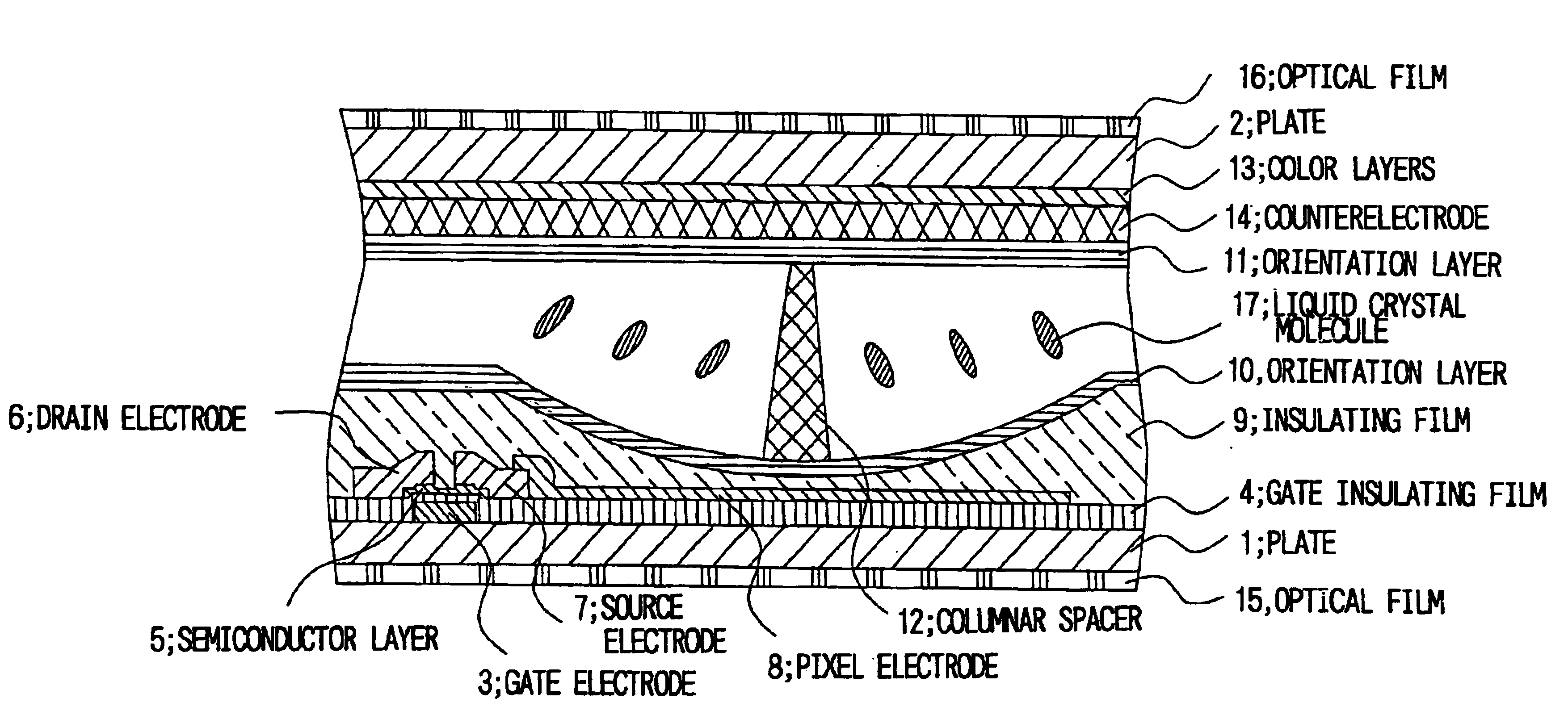
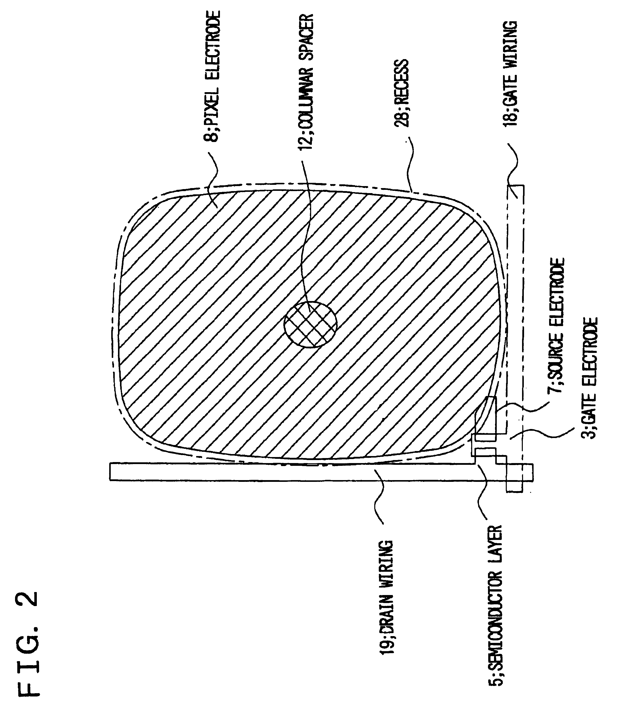
A liquid crystal display device according to a first embodiment of the present invention will be described with reference to FIGS. 1 to 3, in which FIG. 1 is a sectional view showing one pixel of a liquid crystal display device according to the first embodiment, FIG. 2 a plan view of the one pixel and FIG. 3 a sectional view showing one pixel of a liquid crystal display device in which the shape of the curved surface of an orientation layer differs from that of FIG. 1.

A method of manufacturing the liquid crystal device of the first embodiment will be described with reference to FIGS. 1 and 2. First, a gate electrode 3 and gate wiring 18, which comprise a single layer or multiple layers of a metal such as Cr or ITO, are formed on the transparent plate 1 such as glass by a process such as sputtering and a photoresist step, and a gate insulating film 4 comprising the two layers of silicon oxide and silicon nitride is formed on the gate electrode and gate wiring by a process such as CVD...

second embodiment

The second embodiment differs from the first embodiment in that the pixel electrode 8 is provided on the insulating film 9 and basically defines the shape of a recess; wiring 20 is an electrically conductive film, preferably a transparent film so as not to block transmitted light, formed by a process such as sputtering and a photoresist step (here, using ITO) so as to electrically communicate the source electrode 7 and pixel electrode 8; a film which orients the liquid crystal molecules perpendicular to the horizontal plane of the plates is adopted as an orientation layer 21 (and is formed, here, by oblique vapor deposition of SiO); and the direction of inclination of the side surface (wall) of the columnar spacer 12 is such that the cross section of the columnar spacer 12 narrows in the direction toward the plate 1.

According to this arrangement, the pixel electrode 8 generally makes up or defines a recess. As a result, the electric field produced at application of voltage is not pe...


PUM


Abstract

A multi-domain alignment liquid crystal display device in which liquid crystal molecules are aligned through a simple process and panel gap is maintained in stable fashion includes a first plate having a thin-film transistor provided at each point of intersection of a scanning line and signal line, a pixel electrode connected to the thin-film transistor and a first orientation layer formed on the pixel electrode and defining a curved surface, and a second plate having RGB color layers, an counterelectrode provided so as to oppose the pixel electrode, and a second orientation layer. A columnar spacer for regulating the panel gap is provided between the two opposing plates and liquid crystal is sandwiched between the two plates and subjected to multi-domain alignment by the first orientation layer having the curved surface and the columnar spacer.

Description

This invention relates to a liquid crystal display device and, more particularly, to a liquid crystal display device of the "divided alignments type", generally termed as multi-domain alignment (particularly, multi-domain-vertical-alignment) in which, by aligning the liquid crystal molecules differently in each domain within a single pixel, the visual-angle characteristics of the respective domains compensate for each other to provide a wide viewing-angle characteristic.Widely known examples of liquid crystal display devices include those of the twisted nematic (TN) type and those which employ electrically-controlled birefringence (ECB). However, a problem with these conventional devices is that since the alignments of the liquid crystal molecules aligning under application of a voltage are uniform within a pixel, tonality differs depending upon the angle of view. A technique (multi-domain alignment) through which the directions of alignment of liquid crystal molecules in a single p...

Claims


Application Information

Patent Timeline
IPC IPC(8): G02F1/13G02F1/1337G02F1/1339G02F1/1333B66F9/24B66F11/04G02F1/136G02F1/1368
CPCG02F1/13394G02F1/133371G02F1/133707G02F1/133734G02F1/133753G02F2001/133742G02F1/133742G02F1/1337
Inventor MATSUYAMA, HIROAKI
Owner GOLD CHARM LTD
Why Eureka
Try Eureka