

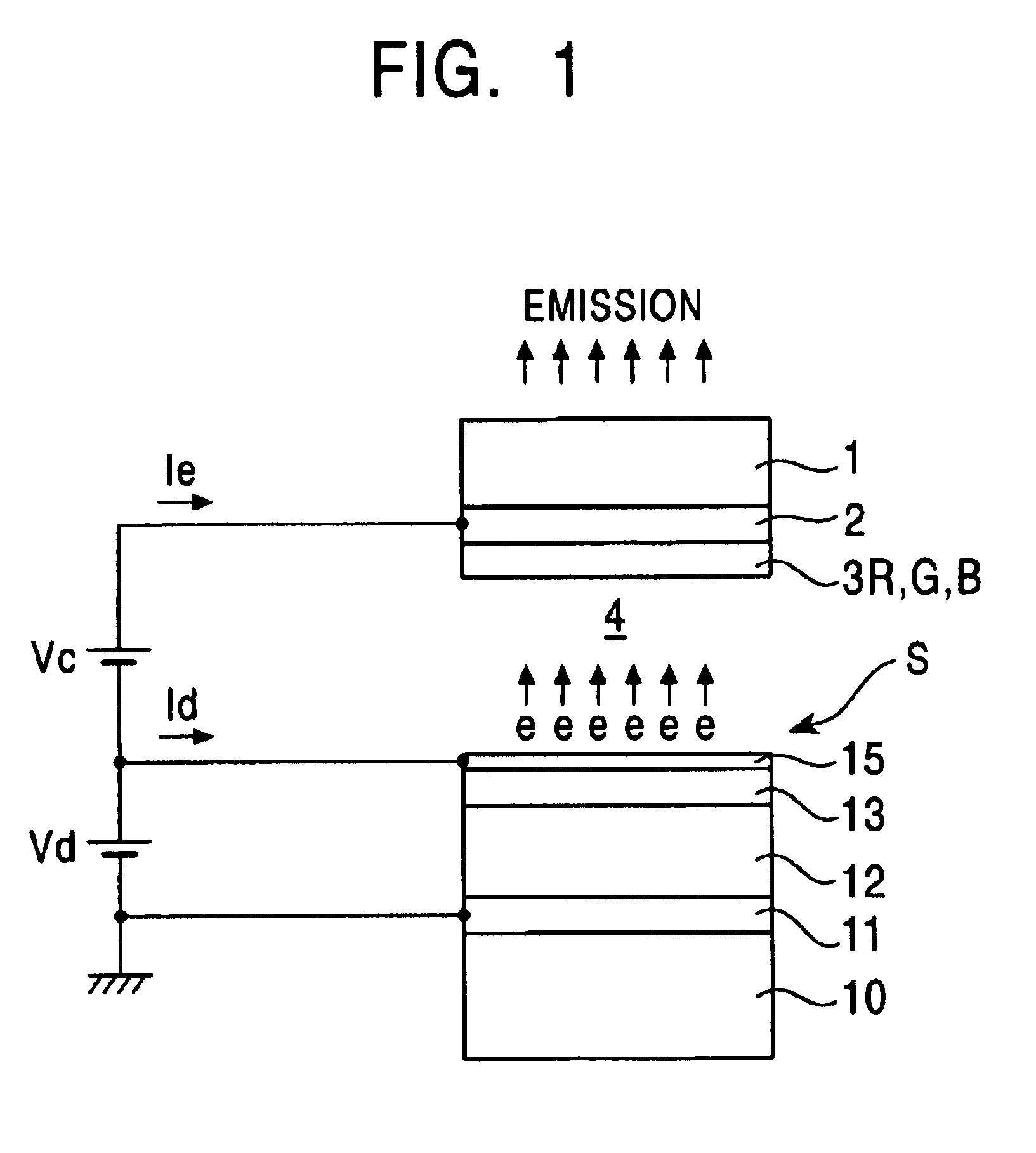
Display device of flat panel structure with emission devices of matrix array
a technology of matrix array and display device, which is applied in the direction of tubes with screens, identification means, instruments, etc., can solve the problems of undesirable electrode pickup sections, a large amount of time and labor, and a large difficulty in the adjustment of the tones and luminance of respective panels in the system, so as to avoid the breakage of the bus electrod
- Summary
- Abstract
- Description
- Claims
- Application Information
AI Technical Summary
Benefits of technology
Problems solved by technology
Method used
Image

Examples
Embodiment Construction
flat panel display device was actually fabricated with specifications (1) through (6) as shown below using a sputtering process for film formation and then characteristics of the same were examined.
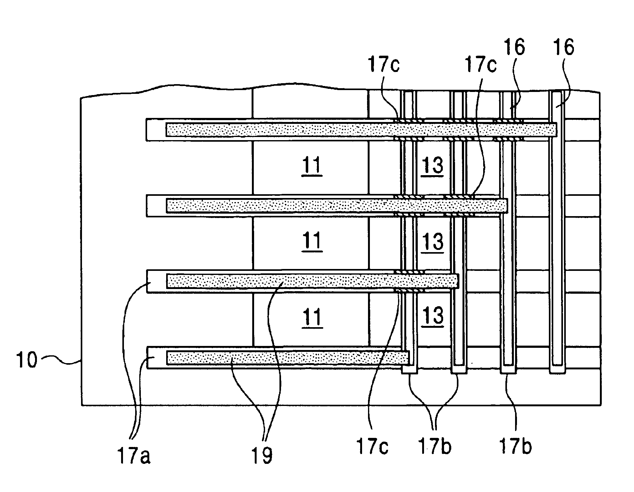
(1) Bottom electrodes: Cr, Cu, and Cr films having thicknesses of 50 nm, 1 .mu.m, and 100 nm, respectively.
(2) Semiconductor electron supply layer: Si layer having a thickness of 4 .mu.m.
(3) Insulator layer: SiO.sub.x layer having a thickness of 330 nm.
(4) Top electrode: Pt film having a thickness of 40 nm.
(5) Bus electrodes: Cr, Cu, and Cr films having thicknesses of 50 nm, 1 .mu.m, and 100 nm, respectively.
(6) Second external repeating terminals: Cr, Cu, and Cr films having thicknesses of 50 nm, 1 .mu.m, and 100 nm, respectively.
(7) First, second, and third insulating protective films: SiO.sub.x films having a thickness of 350 nm.
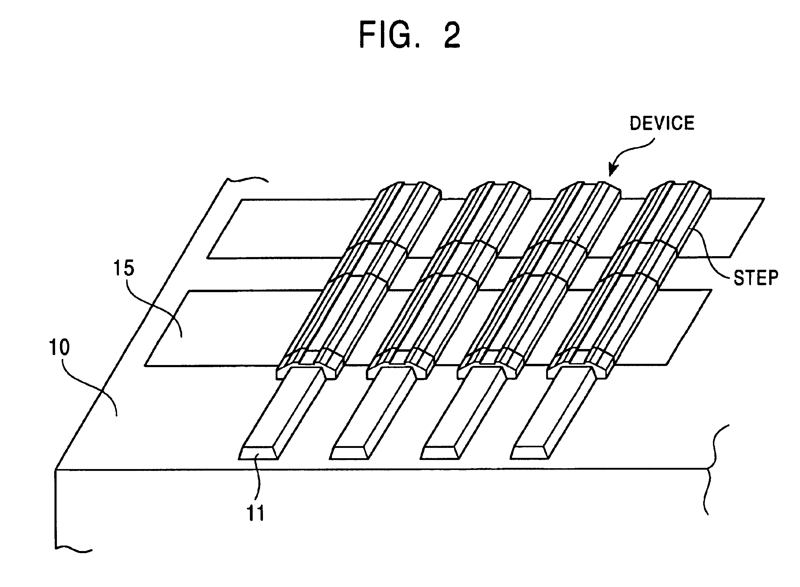
The bottom electrodes (1) and semiconductor electron supply layers (2) were formed in the form of lines on a glass substrate which had been cleaned. Thereafter...
PUM
 Abstract
Description
Claims
Application Information