Semiconductor memory device with memory cells operated by boosted voltage

a memory cell and semiconductor technology, applied in semiconductor devices, digital storage, instruments, etc., can solve the problems of inability to read, consume extra electric power required for charge and discharge of power supply lines, and take a long time for the power supply voltage vddm of the memory cell array

Inactive Publication Date: 2004-09-21
RENESAS ELECTRONICS CORP
View PDF8 Cites 192 Cited by
  • Summary
  • Abstract
  • Description
  • Claims
  • Application Information

AI Technical Summary

Problems solved by technology

However, when the threshold voltage of the MOS transistor in the memory cell of a SRAM has been reduced, the static noise margin, which is the margin with respect to a noise, is reduced, resulting in an unstable read operation.
However, with the prior-art method in which a high voltage is applied to the power supply line for the memory cell array only during read operation described above, it takes much time for the power supply voltage Vddm for the memory cell array to change into a desired voltage Vdd' higher than the power supply voltage Vdd for the peripheral circuits.
Further, an extra electric power required for charge and discharge of the power supply line is consumed for increasing and decreasing the voltage of the power supply line for the memory cell array.
Accordingly, although this circuit is a SRAM circuit operating at a low voltage, it becomes incapable of implementing the lower power consumption.
Even when only the power supply voltage Vddm for the selected memory cell for executing the read operation is boosted, the power consumption is increased to one degree or another.
This eventually requires the relative increase and decrease in voltage between power supply lines, so that the extra electric power required for charge and discharge of the power supply lines is consumed.
Hei 2000-28401, with the method in which the gate width ratio W1 / W3 of 1 is achieved by the change in manufacturing process, for example by changing the impurity concentration of the driving force, and thereby increasing the cell ratio, unfavorably, the manufacturing conditions become complicated, resulting in a reduction of yield, and the number of manufacturing steps is increased, incurring a rise in cost.
There is a problem that the noise margin during write operation is reduced when the power supply voltage Vddm for the memory cell array is boosted regardless of the write or read operation.
Further, although the variations in manufacturing have been reduced, and the required operational margin has been reduced, there is also a possibility that the operational margin during write operation enough for the circuit operation cannot be actually obtained.
As a result, the conductance of the driver MOS transistors N1 and N2 becomes larger than the conductance of the transfer MOS transistors N3 and N4, resulting in an increase in noise margin of the SRAM memory cell.
With this method, the power supply voltage Vddm for the memory cell is required to be boosted and stepped down repeatedly for every operation, resulting in an increase in power consumption.
As a result, the conductance of the driver MOS transistors N1 and N2 becomes larger than the conductance of the transfer MOS transistors N3 and N4, resulting in an increase in noise margin of the SRAM memory cell.
This results in an increase in noise margin of the SRAM memory cell.

Method used


Image

  • Semiconductor memory device with memory cells operated by boosted voltage
  • Semiconductor memory device with memory cells operated by boosted voltage
  • Semiconductor memory device with memory cells operated by boosted voltage

Examples


Embodiment Construction

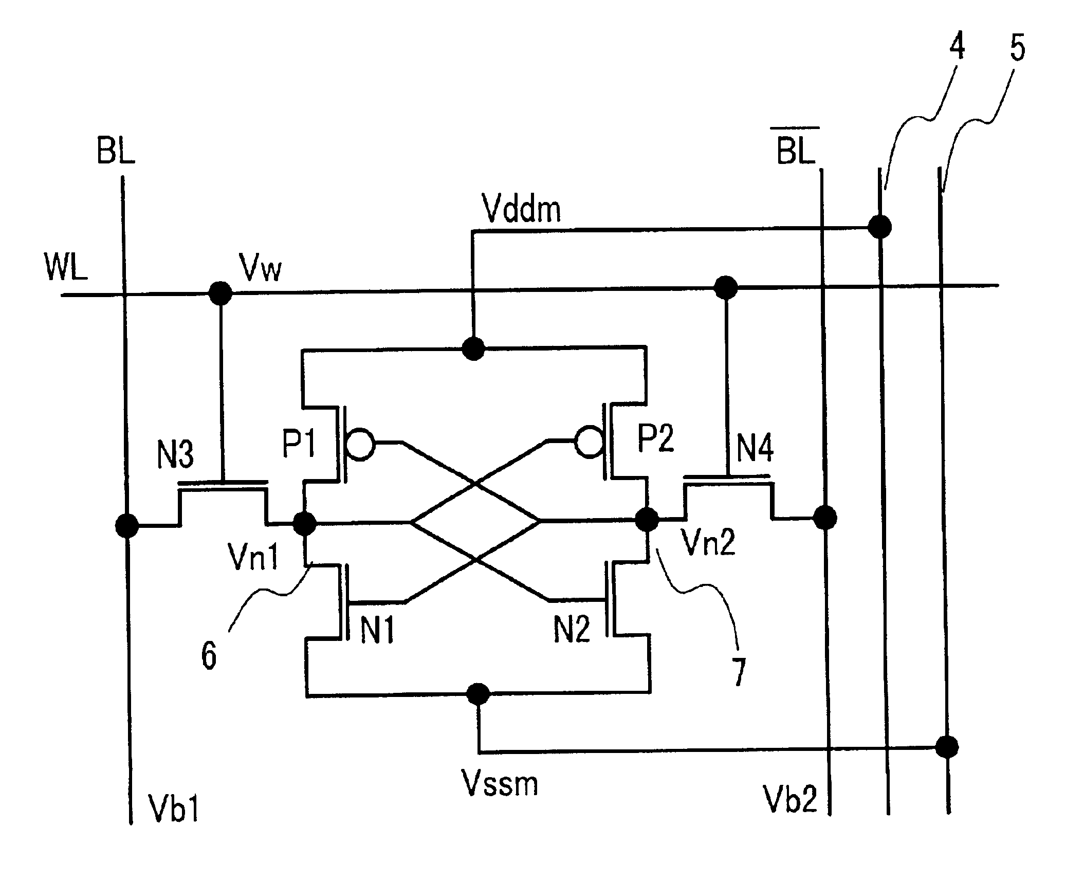
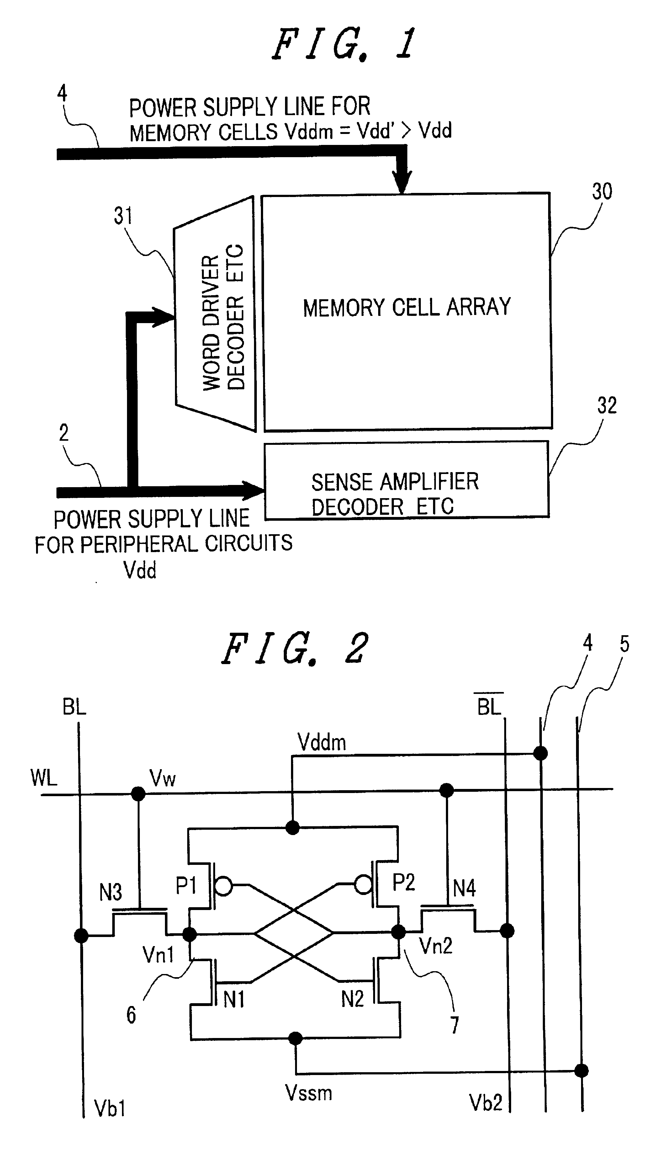
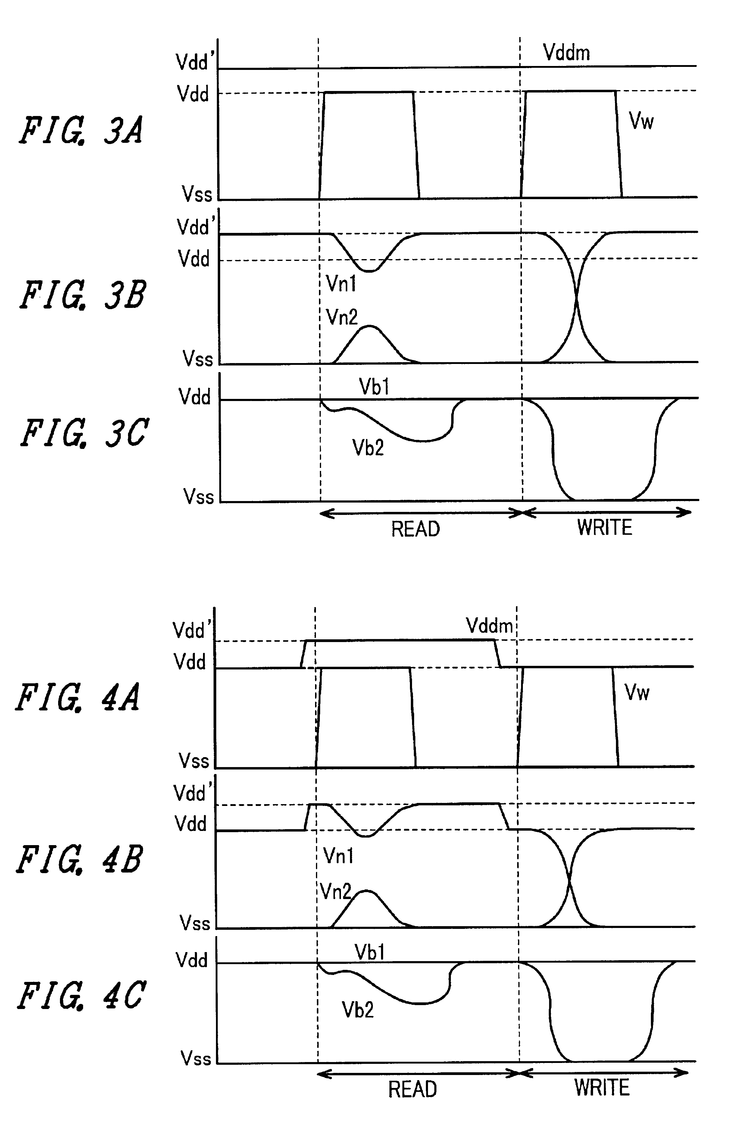
FIGS. 18A and 18B are diagrams respectively showing the voltages to be applied to the SRAM memory cells during the active state and during the non-active state of the SRAM circuit. FIG. 18A shows the power supply voltage Vddm for memory cells and the voltage Vbp of the N-well power supply line. Whereas, FIG. 18B shows the ground voltage Vssm for memory cells and the voltage Vbn of the P-well power supply line 8.

In this power supply voltage application pattern example, during the active state, the voltage Vdd' higher than the power supply voltage Vdd for the peripheral circuits is applied as the power supply voltage Vddm for memory cells and the voltage Vbp of the N-well power supply line. During the non-active state, the voltage Vdd equal to the power supply voltage for the peripheral circuits is applied as both the voltages. As the ground voltage Vssm for memory cells and the voltage Vbn of the P-well power supply line, the constant ground voltage Vss is applied at all times irresp...


PUM


Abstract

A memory using an SRAM memory cell intended for low-voltage operation is designed to decrease the threshold value of MOB transistors constituting the memory cell without substantial decrease in the static noise margin, which is the operational margin of the memory cell. To this end, a voltage Vdd' higher than a power supply voltage Vdd of a power supply line for peripheral circuits is supplied from a power supply line for memory cells as a power supply voltage for memory cells. Since the conductance of driver MOB transistors is in-creased, the threshold voltage of the MOB transistors within the memory cells can be reduced without reducing the static noise margin. Further the ratio of width between the driver MOS transistor and a transfer MOB transistor can be set to 1, thereby allowing a reduction in the memory cell area.

Description

1. Field of the InventionThe present invention relates to a semiconductor memory device. More particularly, it relates to a semiconductor memory device preferable for a SRAM (Static Random Access Memory) which has secured the operational margin during write operation, and operates at a low voltage and a low electric power.2. Description of the Related ArtIn recent years, there has been an increasingly growing trend towards portable devices, which increases a demand for lower power consumption of a large-scale semiconductor integrated circuit (LSI). Therefore, a technology of an LSI operating at a voltage of not more than 1 V becomes necessary. In the future, presumably, there will be growing demands for a further decrease in supply voltage from that of an LSI operating at a supply voltage of about 0.9 V, so that an LSI operating even at a supply voltage of about 0.5 V will be demanded.For operating the LSI at a low voltage, the decrease in threshold voltage of a MOS transistor is ac...

Claims


Application Information

Patent Timeline
Patent Type & Authority Patents(United States)
IPC IPC(8): G11C11/412G11C11/417G11C11/41G11C11/413H01L21/8244H01L27/10H01L27/11
CPCG11C11/412G11C11/417Y10S257/903
Inventor YAMAOKA, MASANAOOSADA, KENICHIISHIBASHI, KOICHIRO
Owner RENESAS ELECTRONICS CORP
Why Eureka
Try Eureka