Method of packaging a device with a lead frame, and an apparatus formed therefrom

a technology of lead frame and device, applied in the direction of electrical apparatus, semiconductor device details, semiconductor/solid-state device details, etc., can solve the problems of mechanical damage to the chip, general thinness and fragility, and the packaging technique of conventional semiconductor chips is not ideal for rf or microwave circuits

Inactive Publication Date: 2004-12-07
TELEDYNE DEFENSE ELECTRONICS LLC
View PDF35 Cites 126 Cited by
  • Summary
  • Abstract
  • Description
  • Claims
  • Application Information

AI Technical Summary

Problems solved by technology

Conventional semiconductor chip packaging techniques are not ideal for RF or microwave circuits.
A majority of microwave circuit chips, however, are fabricated from a gallium arsenide (GaAs) substrate, which is generally thin and fragile.
Therefore, when the plastic is molded onto the surface of a GaAs microwave chip, it may damage the chip mechanically.
Because plastic is a dielectric, molding plastic onto the surface of the chip may also have the effect of detuning the circuit.
Another drawback of conventional semiconductor processing techniques is that the leads are typically not designed for controlled impedances.
A further drawback of conventional semiconductor packaging techniques is that the plastic used for the packaging is very lossy at high frequencies, which may cause significant performance degradation in RF and microwave circuits.
Another problem with conventional semiconductor packaging techniques is wire bonding.
This drawback, coupled with the fact that wire bonds cannot be formed with acceptably tight tolerances at such dimensions, often results in unpredictable and / or unacceptable transmission characteristics for microwave devices.
In the microwave industry, however, because of difficulties in matching the orientation of the transmission mode fields for the circuits and the substrate, efforts to incorporate flip chip mounting have been primarily limited to devices employing co-planar waveguide (CPW) structures as the transmission media.
Many, if not most, commercially available MMICs (monolithic microwave integrated circuits), however, are designed for microstrip transmission modes, and are therefore ill suited for CPW transmission structures.
In addition, the CPW structure has the drawback that it typically requires the use of wire bonding to balance the ground strips of the CPW transmission line structure.

Method used


Image

  • Method of packaging a device with a lead frame, and an apparatus formed therefrom
  • Method of packaging a device with a lead frame, and an apparatus formed therefrom
  • Method of packaging a device with a lead frame, and an apparatus formed therefrom

Examples


Embodiment Construction

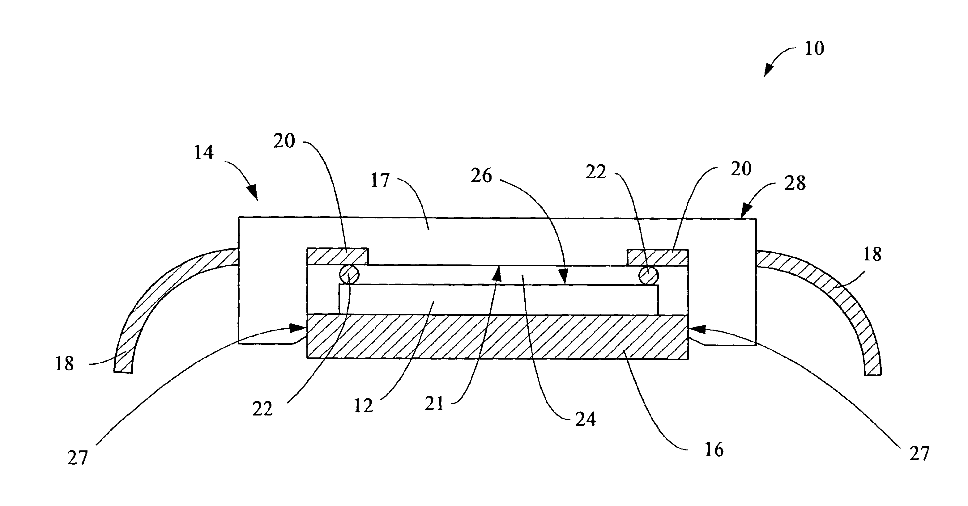
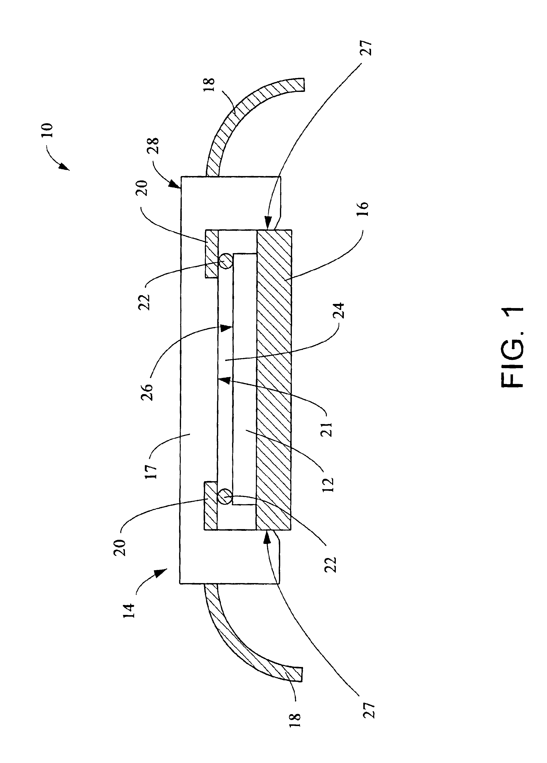
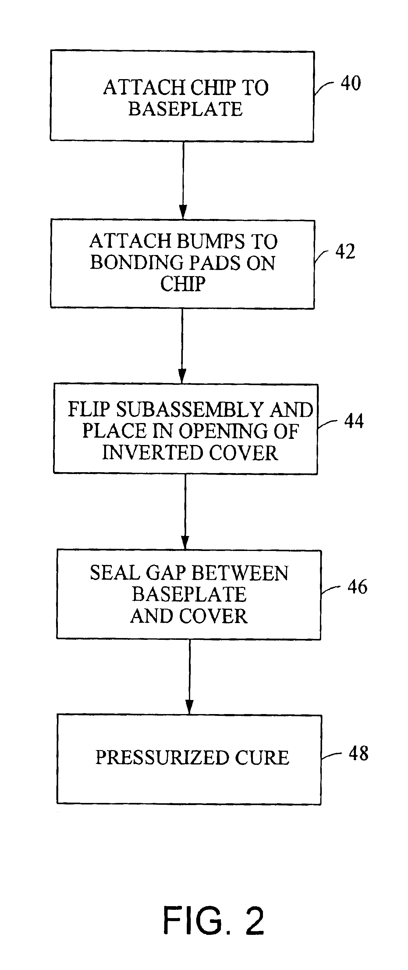
FIG. 1 is a cross-sectional diagram of an apparatus 10 according to one embodiment of the present invention. The apparatus 10 includes a device 12, a cover 14, and a baseplate 16. The cover 14 includes a body 17 and a number of electrically conductive leads 18 captured therein. Although only two are shown in FIG. 1, the apparatus 10 may include as many leads 18 as are necessary to provide the appropriate external connections for the device 12. As described further hereinbelow, the body 17 may be fabricated from injection molded plastic with the leads 18 captured therein, such that a portion 20 of the leads 18 are exposed on the inner surface 21 of the body 17 of the cover 14. In addition, the apparatus 10 includes electrically conductive bumps 22 mounted to the bonding pads of the device 12. The exposed portions 20 of the leads 18 are in electrical contact with the bonding pads of the device 12 via the bumps 22. The resulting air gap 24 between the upper surface 26 of the device 12 ...


PUM


Abstract

A method of packaging a device and an apparatus formed by the method. According to one embodiment, the apparatus includes a base connected to the device, and a cover. The cover includes an injection molded plastic body and at least one electrically conductive lead. The body of the cover is connected to the base such that the device is enclosed by the cover, and the electrically conductive lead includes an exposed portion that is electrically connected to the device.

Description

BACKGROUND OF INVENTION1. Field of InventionThe present invention relates generally to device packaging and, more particularly, to lead frame packaging.2. Description of the BackgroundConventional semiconductor chip packaging techniques are not ideal for RF or microwave circuits. For example, with conventional semiconductor chip packaging techniques, an injection molded plastic package is molded onto the surface of the chip. A majority of microwave circuit chips, however, are fabricated from a gallium arsenide (GaAs) substrate, which is generally thin and fragile. Therefore, when the plastic is molded onto the surface of a GaAs microwave chip, it may damage the chip mechanically. In addition, microwave chips often include air bridges. Because plastic is a dielectric, molding plastic onto the surface of the chip may also have the effect of detuning the circuit. Another drawback of conventional semiconductor processing techniques is that the leads are typically not designed for contro...

Claims


Application Information

Patent Timeline
Patent Type & Authority Patents(United States)
IPC IPC(8): H01L23/31H01L23/28H01L23/58H01L23/66
CPCH01L23/3121H01L23/66H01L2224/16H01L2924/01079H01L2924/01322H01L2924/15311H01L2924/19041H01L2924/3011H01L2924/1423H01L2924/00014H01L2224/0401
Inventor CHEN, TONGCHAI, SUCHET P.
Owner TELEDYNE DEFENSE ELECTRONICS LLC
Why Eureka
Try Eureka