Nanostructure, electron emitting device, carbon nanotube device, and method of producing the same

a carbon nanotube and electron-emitting technology, applied in the field of nanostructure and a method of producing the same, can solve the problem of insufficient uniformity of nanoholes, and achieve the effect of good uniform shape and efficient production of carbon nanotube devices

Inactive Publication Date: 2005-01-04
CANON KK
View PDF17 Cites 109 Cited by
  • Summary
  • Abstract
  • Description
  • Claims
  • Application Information

AI Technical Summary

Benefits of technology

It is still another object of the present invention to provide a method of producing a nanostructure, in a highly reliable fashion, having an anodized film including completely-cut-through nanoholes having good uniformity of shape wherein the anodized film is formed on a substrate including at least one material selected from the group consisting of semiconductors, noble metals, and carbon. It is still another object of the present invention to provide a high-performance electron emitting device capable of emitting a large amount of electrons.
It is still another object of the present invention to provide a method of efficiently producing a carbon nanotube device which can be advantageously used in a high-performance electron emitting device.
The present invention has been achieved based on the knowledge obtained through the experiments performed by the inventors of the present invention. That is, when a thin aluminum film is anodized after forming the thin aluminum film on a substrate having a surface including at least one material selected from the group consisting of semiconductors, noble metals, and carbon, a constant anodization current is observed over a certain period of time and then a reduction in the anodization current occurs. If the anodization is performed while monitoring the anodization current and the anodization is terminated when a particular change in current is detected, it is possible to obtain an anodized film including nanoholes having an uniform shape.

Problems solved by technology

However, a further investigation has revealed that a considerable number of nanoholes produced by the above technique do not reach the electrically conductive surface, and the nanoholes do not have sufficient uniformity in shape.

Method used


Image

  • Nanostructure, electron emitting device, carbon nanotube device, and method of producing the same
  • Nanostructure, electron emitting device, carbon nanotube device, and method of producing the same
  • Nanostructure, electron emitting device, carbon nanotube device, and method of producing the same

Examples


specific embodiments

The present invention is described in further detail below with reference to specific embodiments. It should be understood, however, that the invention is not limited to those embodiments shown here.

first embodiment

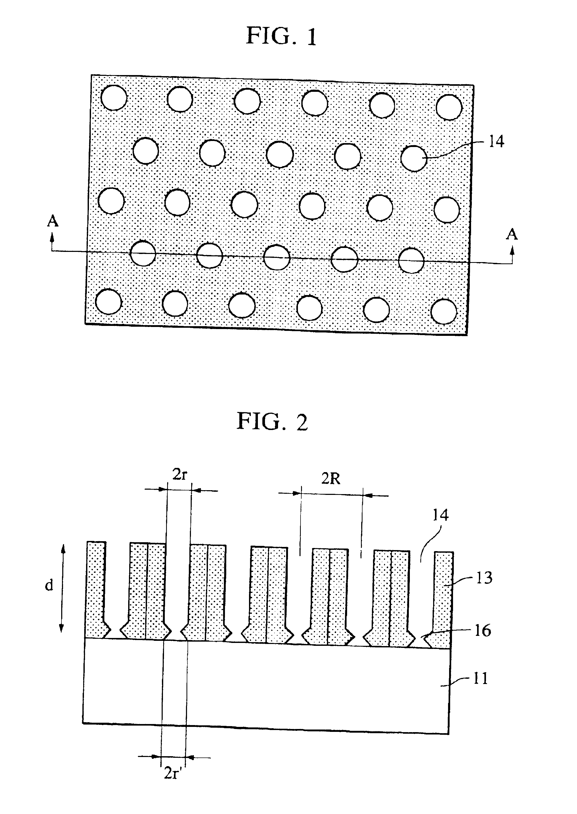
The effects of the anodization time in the process of producing nanoholes by anodizing an aluminum film on a silicon substrate were investigated. The result is described below. In this embodiment, mirror polished single-crystal Si substrates of n-type and p-type having a resistivity of 10−2 Ωcm were used as the Si substrate wherein phosphorus-doped silicon substrates were employed as the n-type substrates and boron-doped silicon substrates were employed as the p-type substrates.

a) Formation of an Al Film on the Si Substrates

An aluminum film with a thickness of 300 nm was formed by means of RF sputtering on the surface of three Si substrates of each type (six wafers in total). The RF sputtering process was performed using Ar gas at 30 mTorr with RF power of 500 W.

b) Anodization

Anodization was performed using the anodization apparatus shown in FIG. 6.

In the present embodiment, a 0.3 M aqueous solution of oxalic acid was used as the electrolyte, and the solution was kept at 17° C. usin...

second embodiment

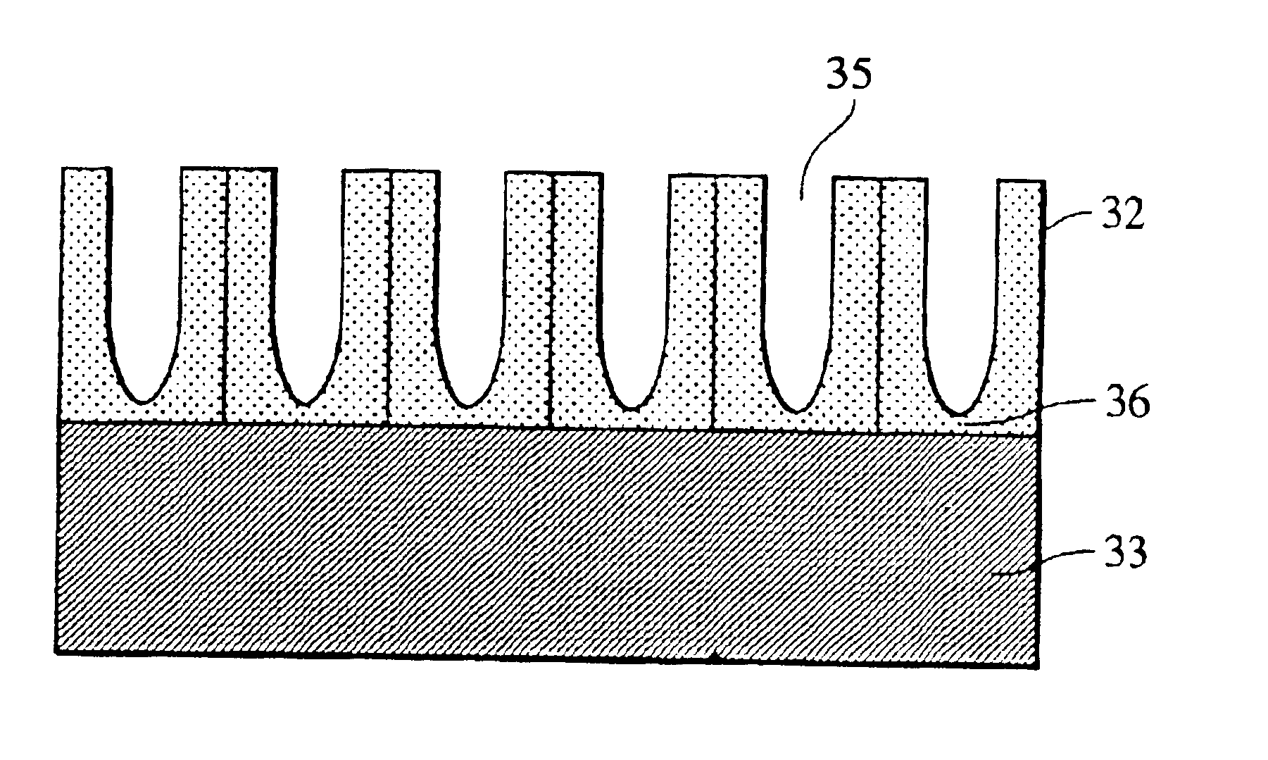
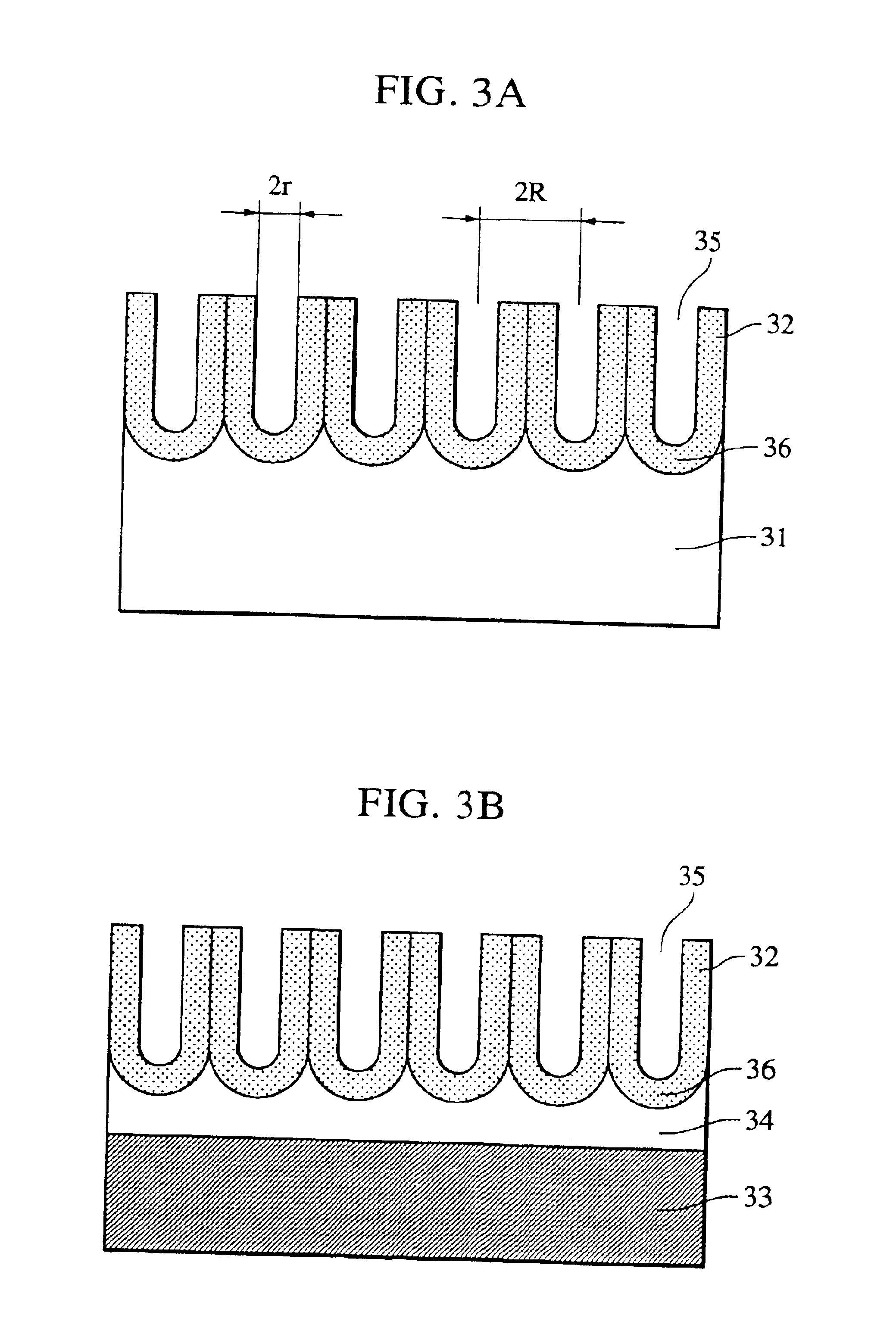
Nanoholes were produced in a similar manner to the first embodiment except that n-type silicon wafers with a resistivity of 0.01 Ωcm were used as the substrate and that the anodization was terminated at point D in FIG. 7.

After producing the nanoholes on the n-type silicon substrate and performing the pore widening process in a similar manner to the first embodiment, Co was electro-deposited thereby forming catalytic fine particles inside the nanoholes. In the above electro-deposition process, a solution consisting of 5% CoSO4.7H2O and 2% H3BO3 was employed as a plating bath and the electro-deposition was performed for 10 sec under application of an AC voltage of 5 V.

One sample was etched by immersing the sample in a 1% aqueous solution of hydrofluoric acid for 10 sec before the electro-deposition process. Another sample was directly subjected to the electro-deposition process without being etched before the electro-deposition process.

The cross section of the samples were observed wi...


PUM

PropertyMeasurementUnit
sizeaaaaaaaaaa
diametersaaaaaaaaaa
diametersaaaaaaaaaa

Abstract

The invention provides a nanostructure including an anodized film including nanoholes. The anodized film is formed on a substrate having a surface including at least one material selected from the group consisting of semiconductors, noble metals, Mn, Fe, Co, Ni, Cu and carbon. The nanoholes are cut completely through the anodized film from the surface of the anodized film to the surface of the substrate. The nanoholes have a first diameter at the surface of the anodized film and a second diameter at the surface of the substrate. The nanoholes are characterized in that either a constriction exists at a location between the surface of the anodized film and the surface of the substrate, or the second diameter is greater than the first diameter.

Description

BACKGROUND OF THE INVENTION1. Field of the InventionThe present invention relates to a nanostructure and a method of producing the same. The nanostructure produced by anodizing aluminum according to the present invention may be used in a wide variety of applications such as functional materials for use in electronic devices or micro devices. Specific examples include quantum effect devices, electrochemical sensors, biosensors, magnetic memories, magnetic devices, light emitting devices, photonic devices, solar cells, etc.2. Description of the Related ArtIn thin films, fine wires, and fine dots of metal or semiconductor, if motion of electrons is restricted within a region smaller than a particular length, the thin films, the fine wires, or the fine dots often exhibit special electric, optical, and / or chemical characteristics. From this point of view, materials having a fine structure (nanostructure) with a size smaller than 100 nm are attracting increasing attention as functional ma...

Claims


Application Information

Patent Timeline
Patent Type & Authority Patents(United States)
IPC IPC(8): B81C1/00G01N27/403G01N27/414G11B5/855G11B5/73H01F1/00G11B5/62H01J1/304B82B3/00H01J9/02H01L21/3063
CPCB81C1/00087B82Y10/00B82Y25/00G11B5/7325G11B5/743G11B5/855H01F1/0081H01F1/009H01J1/304H01J1/3042H01J9/025Y10S977/78G11C2213/81H01J2201/30469Y10S977/778Y10S977/939B81C2201/0114G11B5/739
Inventor IWASAKI, TATSUYADEN, TOHRU
Owner CANON KK
Why Eureka
Try Eureka