Method of manufacturing semiconductor device and manufacturing apparatus
a manufacturing method and semiconductor technology, applied in the direction of semiconductor/solid-state device manufacturing, electric devices, basic electric elements, etc., can solve the problems of increased dielectric constant in the interlayer insulating film, increased risk of oxidation, and increased risk of dielectric constant as a whole, so as to simplify the manufacturing process
- Summary
- Abstract
- Description
- Claims
- Application Information
AI Technical Summary
Benefits of technology
Problems solved by technology
Method used
Image

Examples
Embodiment Construction
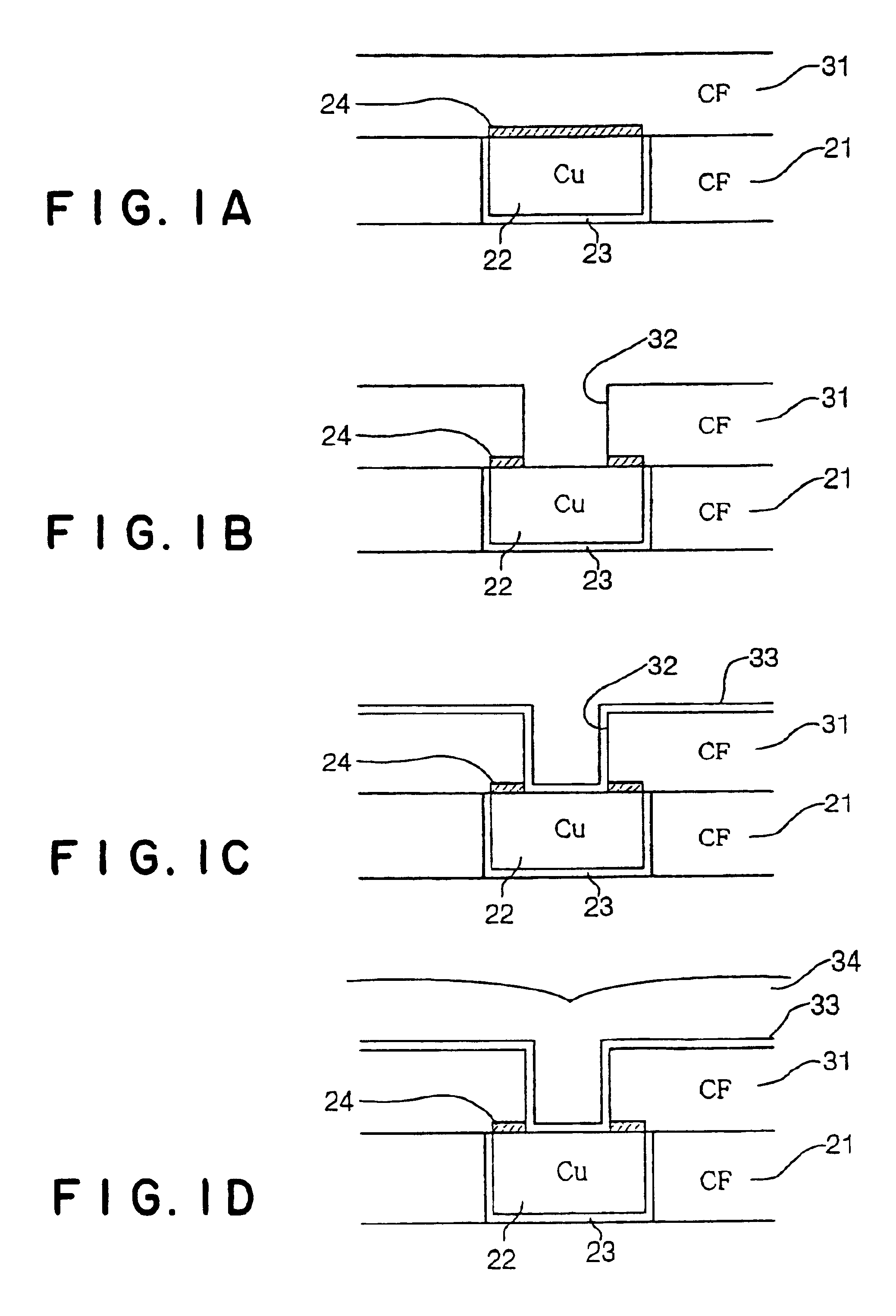
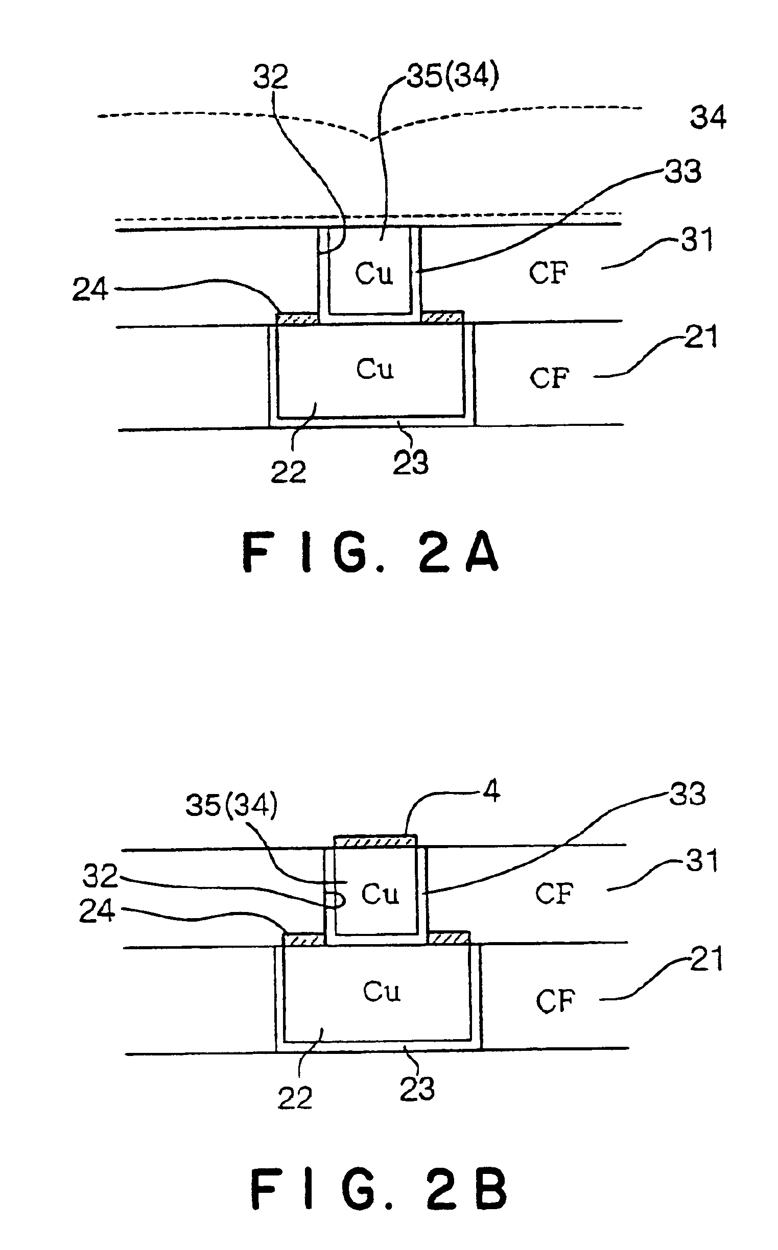
A preferred embodiment of the manufacturing method of semiconductor devices according to the present invention will be described, focusing on an example of a single damascene process for simplifying the description, with reference to FIGS. 1A, 1B, 1C, 1D, 2A and 2B.
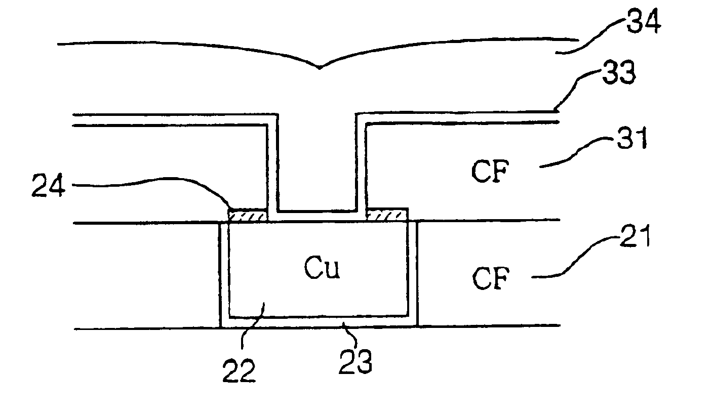
FIGS. 1A through 1D illustrate process steps of making through-holes above wiring (metal layer) which extends in circuitry at the n-th level stacked on the substrate to make wiring line (which is also referred to as “wiring” in this embodiment) which connects to wiring in circuitry at the (n+1)th level. In FIGS. 1A through 1D, reference numeral 21 refers to an insulating film (interlayer insulating film) at n-th level formed of fluorine-contained carbon film (CF film) of a low dielectric constant, for example, 22 to a metal layer serving as wiring and made of copper in circuitry at the n-th level, 23 to a barrier layer preventing copper from diffusing into the insulating film 21, and 24 to a protection film explained late...
PUM
 Abstract
Description
Claims
Application Information