Liquid crystal display device and method of manufacturing the same

a technology of liquid crystal display and liquid crystal, which is applied in static indicating devices, instruments, non-linear optics, etc., can solve the problems of light leakage, pixel electrode charge leakage, and reducing the driving voltage of liquid crystal

Inactive Publication Date: 2005-01-04
SEMICON ENERGY LAB CO LTD
View PDF15 Cites 92 Cited by
  • Summary
  • Abstract
  • Description
  • Claims
  • Application Information

AI Technical Summary

Benefits of technology

[0014]The present invention has been made to solve the foregoing problems, and therefore has an object of the present invention to provide a novel liquid crystal display device comprising a reflection layer in which incident light is reflected more efficiently, and a method of manufacturing the same.

Problems solved by technology

Therefore, a problem of a so-called light leak phenomenon occurred in which a reduced off resistance of the switching elements 11, occurrence of a photo carrier, and the like causes charges of the pixel electrodes to leak, thereby reducing a liquid crystal driving voltage.
Since the conventional reflection layer (pixel electrodes made of a metal material) does not provide a sufficient reflection and irregular reflection of light, there is a problem with a brightness suitable for a liquid crystal display device (in particular, a direct-vision-type reflection type liquid crystal panel).
Also, in the conventional reflection layers (pixel electrodes), gaps between adjacent reflection layers (pixel electrodes) are large, thereby causing the light leak.
Further, conventionally, such a problem has been arisen in which the reflectivity of the refection layer is lowered due to formation of an orientated layer with a high refractive index on the reflection layer (electrodes made of a metal material).
Alternatively, when silver is used as a metal material, a silver electrode having the reflectivity as high as 97.6% is liable to be oxidized.
Thus, the silver is difficult to be employed because of being difficult to be processed.

Method used


Image

  • Liquid crystal display device and method of manufacturing the same
  • Liquid crystal display device and method of manufacturing the same
  • Liquid crystal display device and method of manufacturing the same

Examples


embodiment 1

[0157

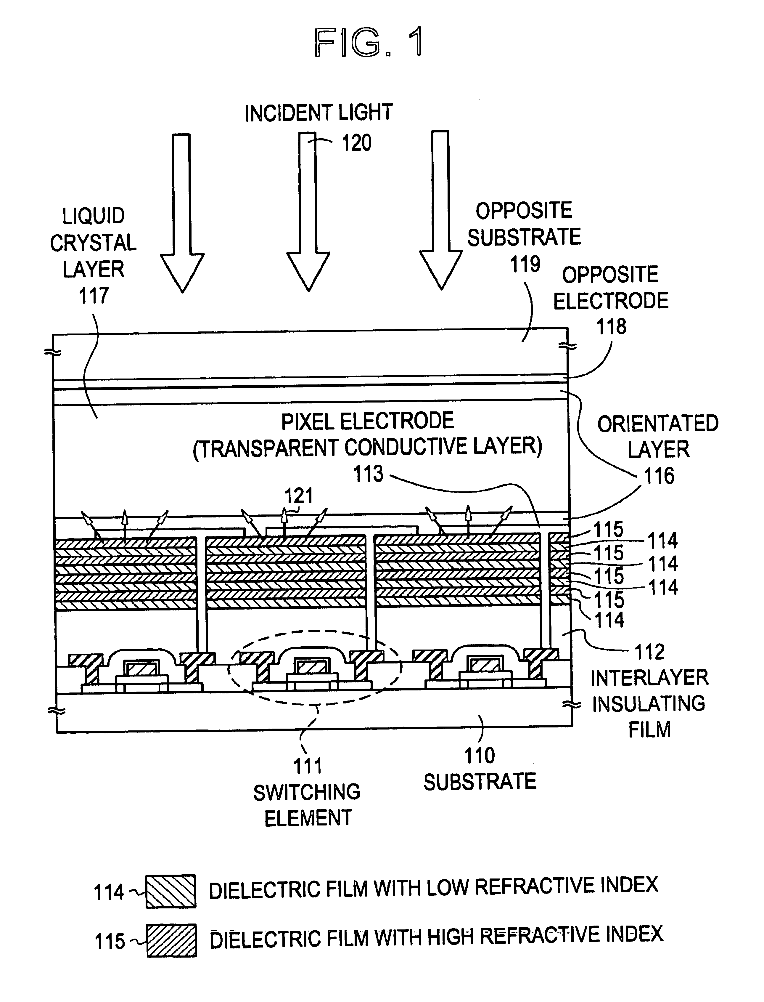
[0158]In the present embodiment, a process example for forming a pixel matrix circuit of a reflection type LCD using the present invention is described with reference to FIGS. 3A to 3D and 4A to 4C. Incidentally, since the present invention is a technique relating to a reflection layer, the structure of a switching element, for example, the structure of a TFT itself is not limited to the present embodiment.

[0159]Initially, a substrate 301 having an insulating surface is prepared. For a substrate, a glass substrate, a quartz substrate, a ceramics substrate, a semiconductor substrate may be used. Next, an underlying film (not shown) is formed on the substrate. For the underlying film, a silicon oxide film, a silicon nitride film, a silicon nitride oxide film may be used in a film thickness of a rang from 100 nm to 300 nm. In the present embodiment, a TEOS is used for a raw material, and a silicon oxide film is formed in a film thickness of 200 nm. It is to be noted that if it is ...

embodiment 2

[0192

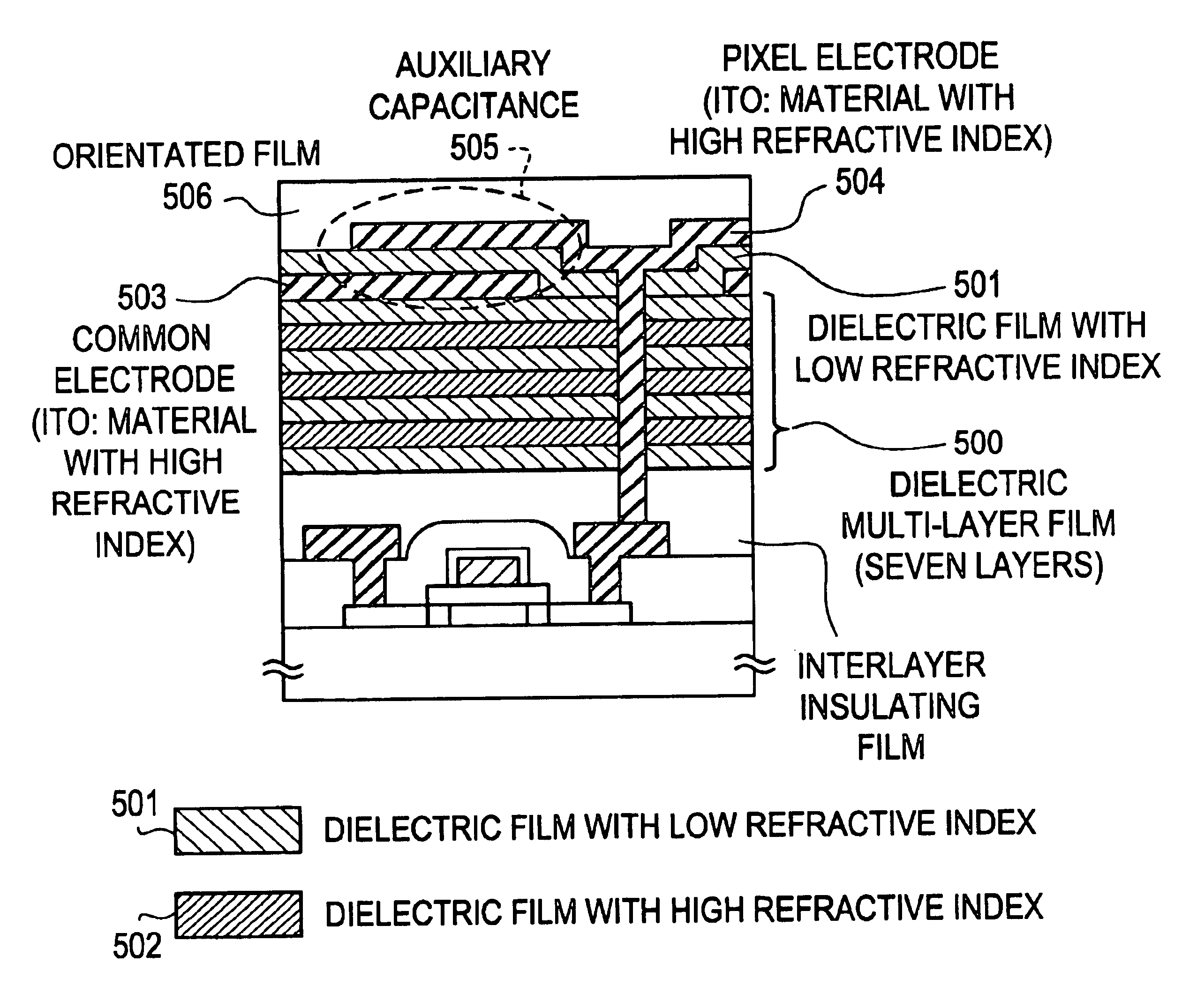
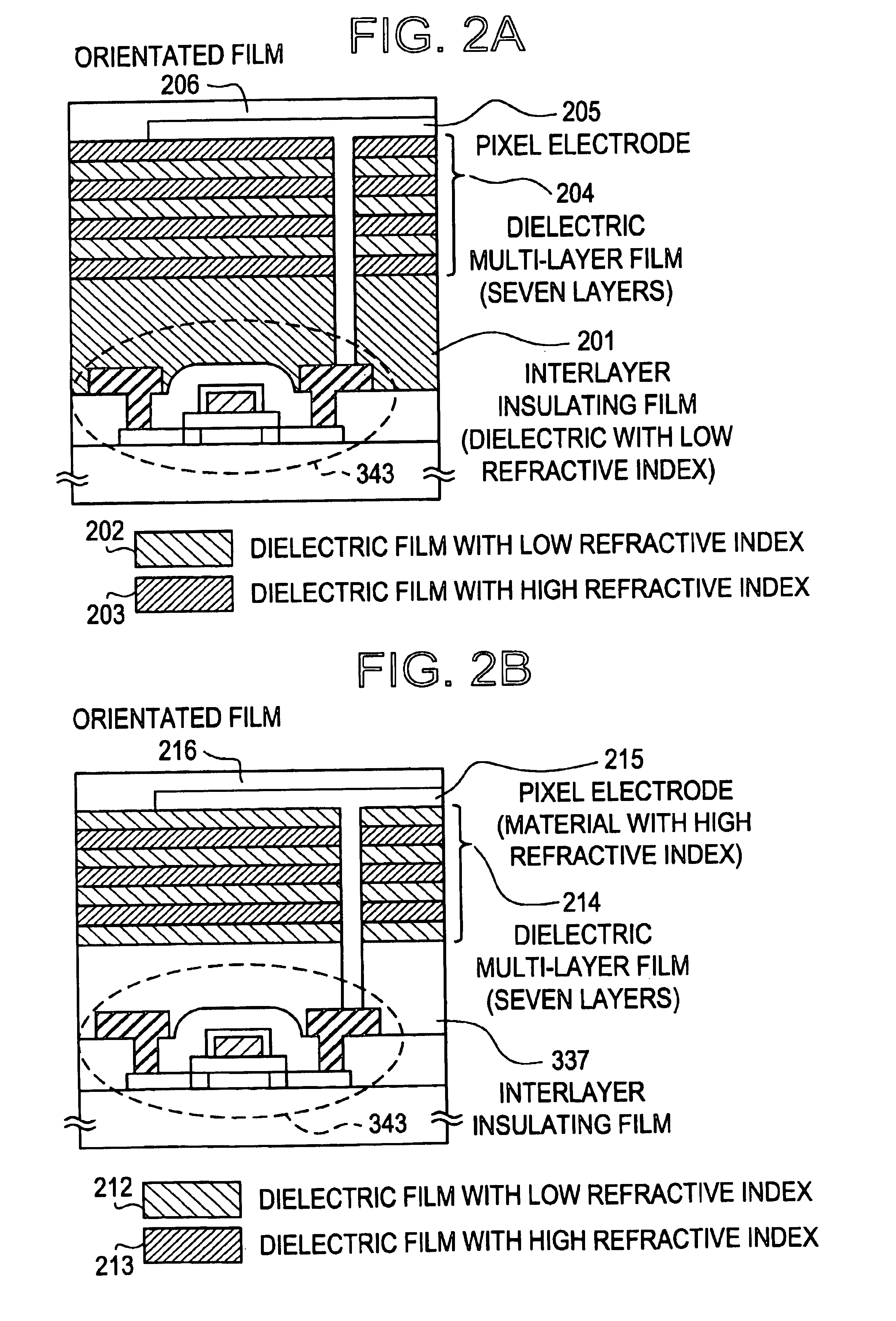
[0193]In Embodiment 1, an example of the fabrication process is described in which a dielectric multilayer film consisting of eight layers is formed. A description will now be made of the present embodiment with reference to FIG. 2A, in which a dielectric material with a low refractive index is used as a second interlayer insulating film 337 to form a dielectric multilayer film consisting of seven layers. Until a process shown in FIG. 3C, the fabrication process is the same as that of the reflection type LCD shown in Embodiment 1. Therefore, only different portions will be described.

[0194]First, the structure shown in FIG. 3C is obtained using the same technique as that of the fabrication process shown in Embodiment 1. Then, for the second interlayer insulating film 337, a dielectric material having a low refractive index is used. In the present embodiment, as an interlayer insulating film 201 is formed an acrylic film having a film thickness of 1 μm.

[0195]Incidentally, in the ...

embodiment 3

[0202

[0203]In Embodiment 1, an example of the fabrication process is described in which a dielectric multilayer film consisting of eight layers is formed. The present embodiment will be described with reference to FIG. 2B, in which a seven-layer dielectric multilayer film is formed, on which a pixel electrode is formed using a material having a high refractive index. Incidentally, until a process shown in FIG. 3C, the fabrication process is the same as that of the reflection type LCD shown in Embodiment 1. Therefore, only different portions will be described.

[0204]First, a structure shown in FIG. 3C is obtained using the same technique as that of the manufacturing process shown in Embodiment 1.

[0205]Then, three sets of a dielectric film 212 with a low refractive index and a dielectric film 213 with a high refractive index, that is, a dielectric film having six layers is formed on a second interlayer insulating film 337. One layer of the dielectric film with a low refractive index is...


PUM

PropertyMeasurementUnit
thicknessaaaaaaaaaa
thicknessaaaaaaaaaa
thicknessaaaaaaaaaa

Abstract

To provide a novel liquid crystal display device comprising a light reflection layer where light is likely to more effectively reflect, and a method of manufacturing the same. The present invention can realize high resolution and high opening rate by using a dielectric multi-layer film as the light reflection layer to form thereon a pixel electrode consisting of a transparent conductive films.

Description

BACKGROUND OF THE INVENTION[0002]1. Field of the Invention[0003]The present invention relates to the structure of an electronic device such as personal computers and word processors, and more specifically, to a liquid crystal display (LCD) device equipped with the electronic device and a method of manufacturing a reflection layer in the liquid crystal display device. The present invention may also be applied to an electro-optical device having the liquid crystal display device.[0004]A “semiconductor device” as used herein refers to a general device activated by a semiconductor. Therefore, the above-noted liquid crystal display device and the electro-optical device also fall within a category of semiconductor device. For clarification, the terms of “liquid crystal display device” and “electro-optical device” are separately used herein.[0005]2. Description of the Related Arts[0006]Typically, a reflection type liquid crystal display device is known. The reflection type liquid crystal d...

Claims


Application Information

Patent Timeline
Patent Type & Authority Patents(United States)
IPC IPC(8): G02F1/1335G02F1/13
CPCG02F1/133553G02F1/133502
Inventor HIRAKATA, YOSHIHARUSATAKE, RUMOKUWABARA, HIDEAKINISHI, TAKESHI
Owner SEMICON ENERGY LAB CO LTD
Why Eureka
Try Eureka