Method for manufacturing a multi-layer printed circuit board

a printed circuit board and multi-layer technology, applied in the direction of printed circuit aspects, printed element electric connection formation, conductive pattern formation, etc., can solve the problems of increased pcb size, inefficient routing of signal traces on signal layers, and difficulty in laying down traces, so as to facilitate the routing of signal traces

a printed circuit board and multi-layer technology, applied in the direction of printed circuit aspects, printed element electric connection formation, conductive pattern formation, etc., can solve the problems of increased pcb size, inefficient routing of signal traces on signal layers, and difficulty in laying down traces, so as to facilitate the routing of signal traces

US6839964B2Inactive Publication Date: 2005-01-11FORMFACTOR INC

Image

  • Method for manufacturing a multi-layer printed circuit board
  • Method for manufacturing a multi-layer printed circuit board
  • Method for manufacturing a multi-layer printed circuit board

Examples


Embodiment Construction

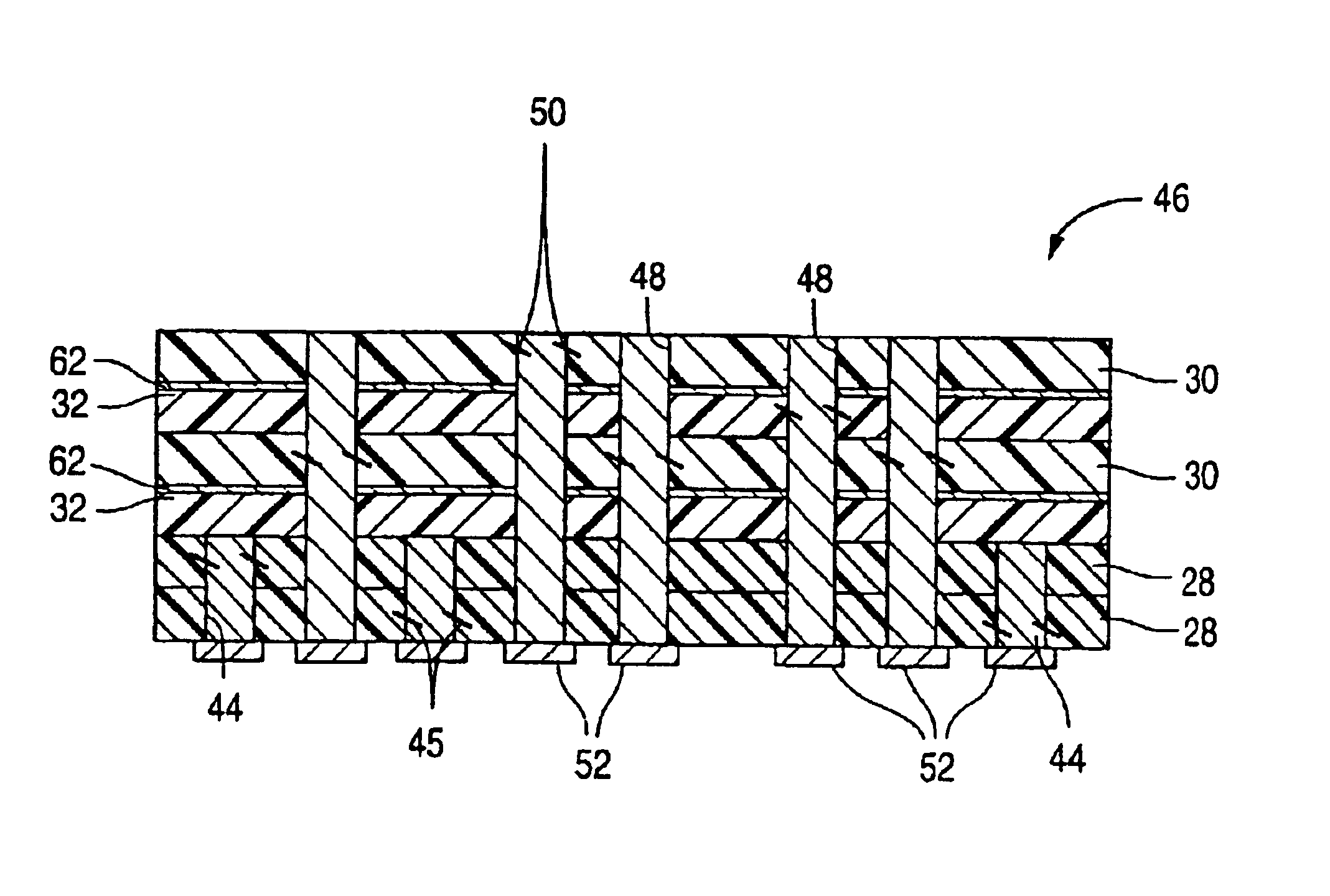
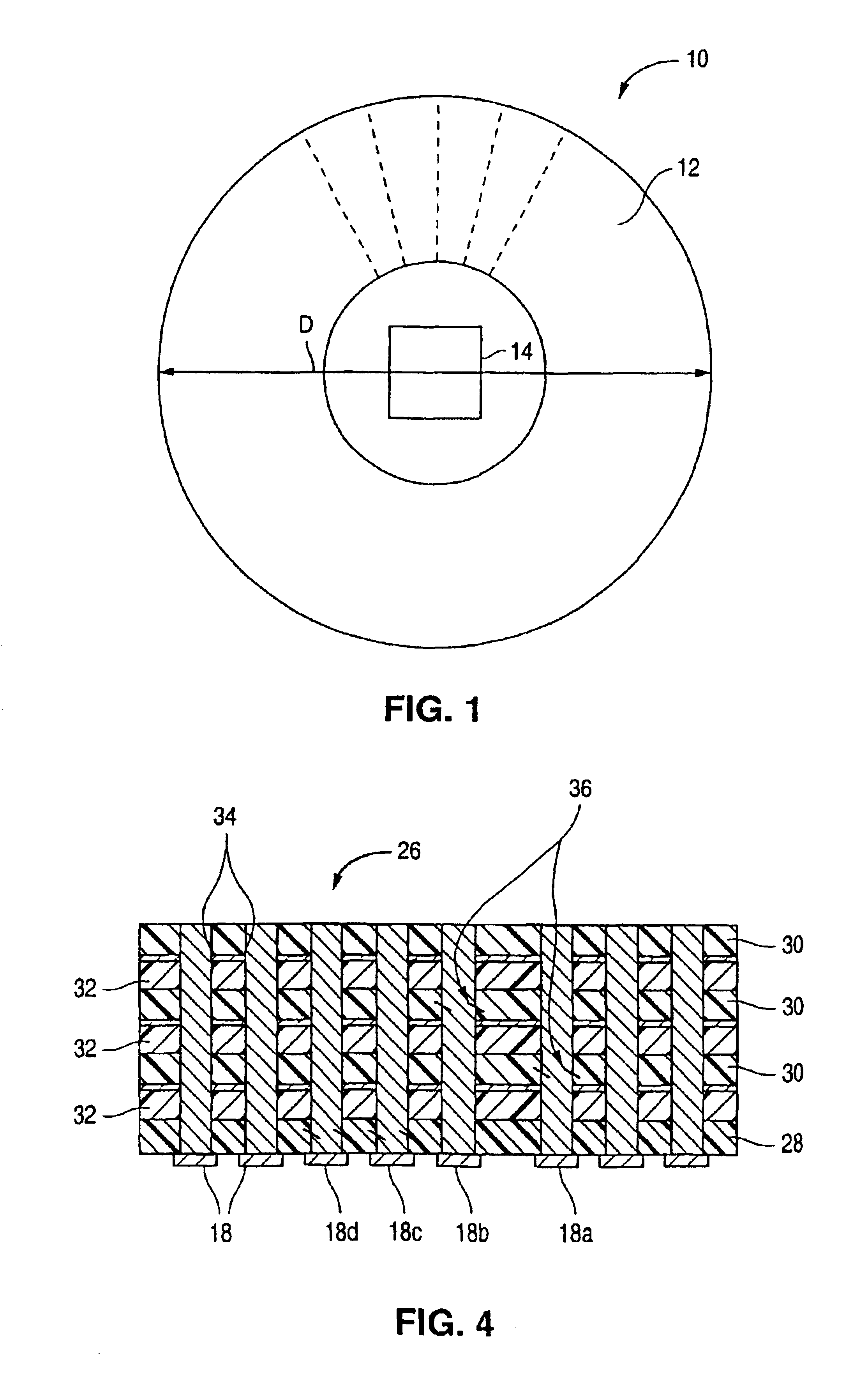
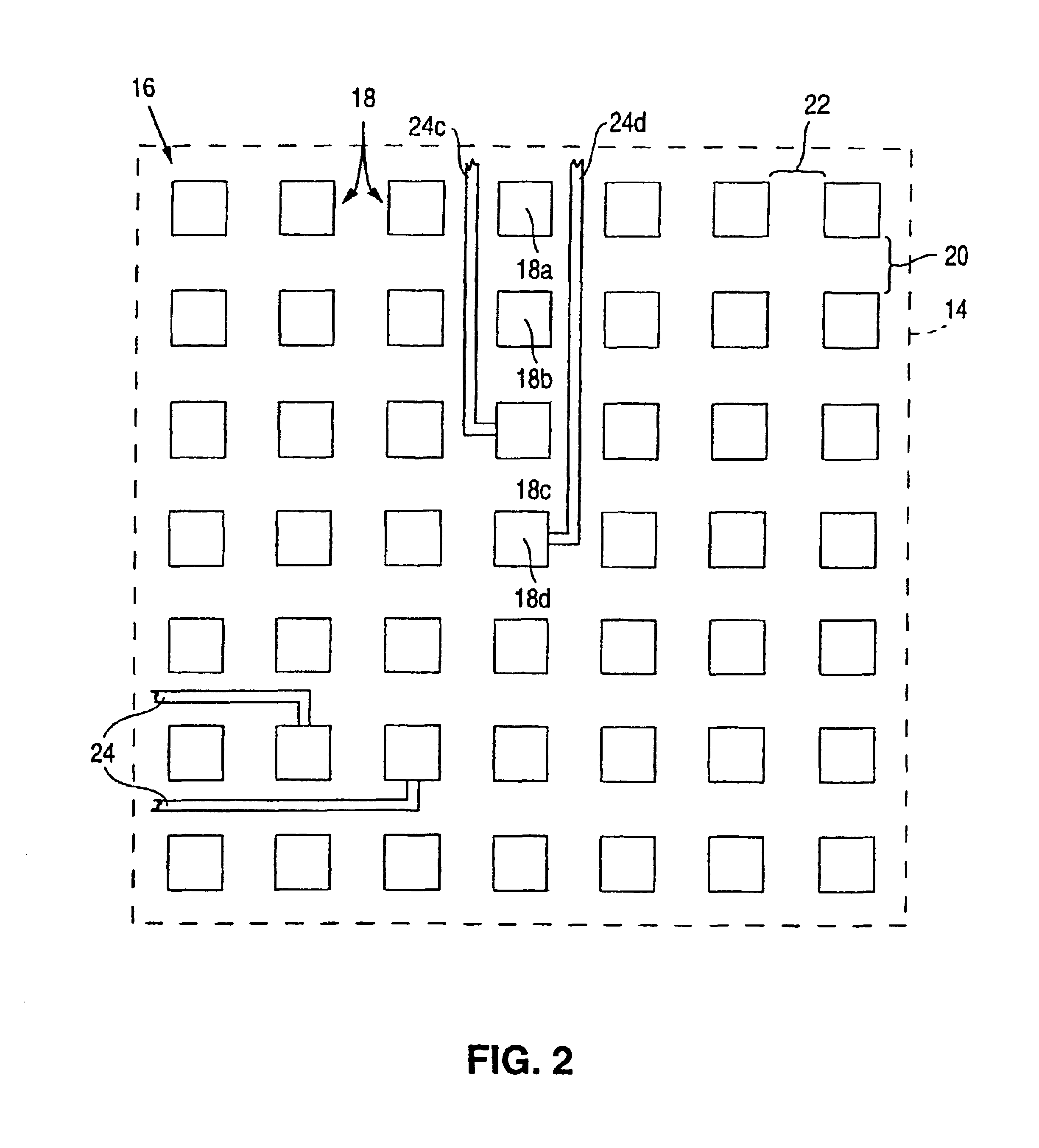
It is to be understood in the following discussion that a description of only an idealized PCB is given for purposes of illustrating the concepts of the invention. An actual multilayer PCB could have far more layers and many more vias than are shown in the following example. Referring to FIGS. 7(A)-7(E), a preferred multilayer PCB manufacturing method of a first embodiment of the present invention is shown. Turning now to FIGS. 7(A) and 8, metalized patterns or regions 54, 60, and 62 are masked onto individual power layers 28, signal layers 30, and ground layers 32, respectively. Although the ground layers 32 are shown as being interspersed between each of the signal layers 30, this need not be the case. Ground layers 32 may be positioned between groups of signal layers, depending upon the circuit design and the need for signal isolation. It also is to be understood that while the regions, traces and contacts are depicted as only being on one side of the PCBs, the regions, traces an...


PUM

PropertyMeasurementUnit
diameteraaaaaaaaaa
diametersaaaaaaaaaa
diametersaaaaaaaaaa

Abstract

A method of manufacturing a multilayer printed circuit board (PCB) is provided, the PCB having blind vias connecting to power layers. A portion of the blind vias in the power layers are grouped together to form a cluster of blind vias. Signal layers, provided separate from the power layers, include signal routing channels, with at least some of the signal routing channels aligned above or below the cluster of blind vias of the power layers.

Description

BACKGROUND OF THE INVENTION1. Field of the InventionThe present invention relates generally to a printed circuit board for use in a probe card for testing a semiconductor wafer, and more particularly, to a multilayer printed circuit board having clustered vias in power layers to facilitate the routing of signal traces in signal layers.2. Description of Related ArtProbe cards are on, or typically include, printed circuit boards (“PCBs”) and are utilized to distribute signals, power, and ground between a remote host tester and a semiconductor device under test (“DUT”) resident on a wafer under test (“WUT”). Typically, thousands of signals are communicated between the remote host tester and the DUTs resident on a WUT. As a result, a signal routing scheme must be incorporated into the design of a probe card's PCB.Referring to FIG. 1, a newly developed probe card 10 of the assignee of the present invention has a diameter “D” of 12 to 18 inches. Signals input along the outer region 12 of ...

Claims


Application Information

Patent Timeline
11 Jan 2005
Publication
US6839964B2
IPC
H05K3/46; H05K1/11; H05K3/42
CPC
H05K1/115; H05K3/4623; H05K3/429; H05K2201/093; H05K2201/09309; Y10T29/49165; H05K2201/09663; H05K1/0262
Inventors
HENSON, ROY