Semiconductor integrated circuit device and imaging system

a technology of integrated circuits and semiconductors, applied in the field of noise reduction techniques in imaging systems, can solve the problems of increased chip size, deterioration of display quality, and noise appearing on the power supply, so as to improve display quality, control the effect of output noise and improved display quality

Inactive Publication Date: 2005-01-11
RENESAS SEMICON PACKAGE & TEST SOLUTIONS +1
View PDF7 Cites 0 Cited by
  • Summary
  • Abstract
  • Description
  • Claims
  • Application Information

AI Technical Summary

Benefits of technology

[0019]According to the means explained above, a through-current in the output circuit of the semiconductor integrated circuit provided with the AD conversion circuit can be reduced, and noise resulting from change of output can also be controlled, and as a result, display quality can be improved.
[0020]It is preferable that the first code conversion means uses a binary gray code conversion circuit for converting a binary code to the gray code, while the second code conversion means uses a gray binary code conversion circuit for converting the gray code to the binary code. Thereby, the number of bits which change whenever the output digital signal is changed over can be surely reduced and the display quality can be improved.
[0021]Moreover, it is also possible to use a circuit for adding a fixe

Problems solved by technology

Therefore, it is thought that noise appears on the power supply because a large current flows when an output signal is changed over.
Moreover, noise generated in the output circuit is also propagated to an internal circuit other than the input circuit via the substrate, but since the AD conversion LSI includes an amplifying circuit such as a PGA (programmable gain amplifier) for amplifying an input analog signal, the noise propagated to the input side is also a

Method used


Image

  • Semiconductor integrated circuit device and imaging system
  • Semiconductor integrated circuit device and imaging system
  • Semiconductor integrated circuit device and imaging system

Examples


second embodiment

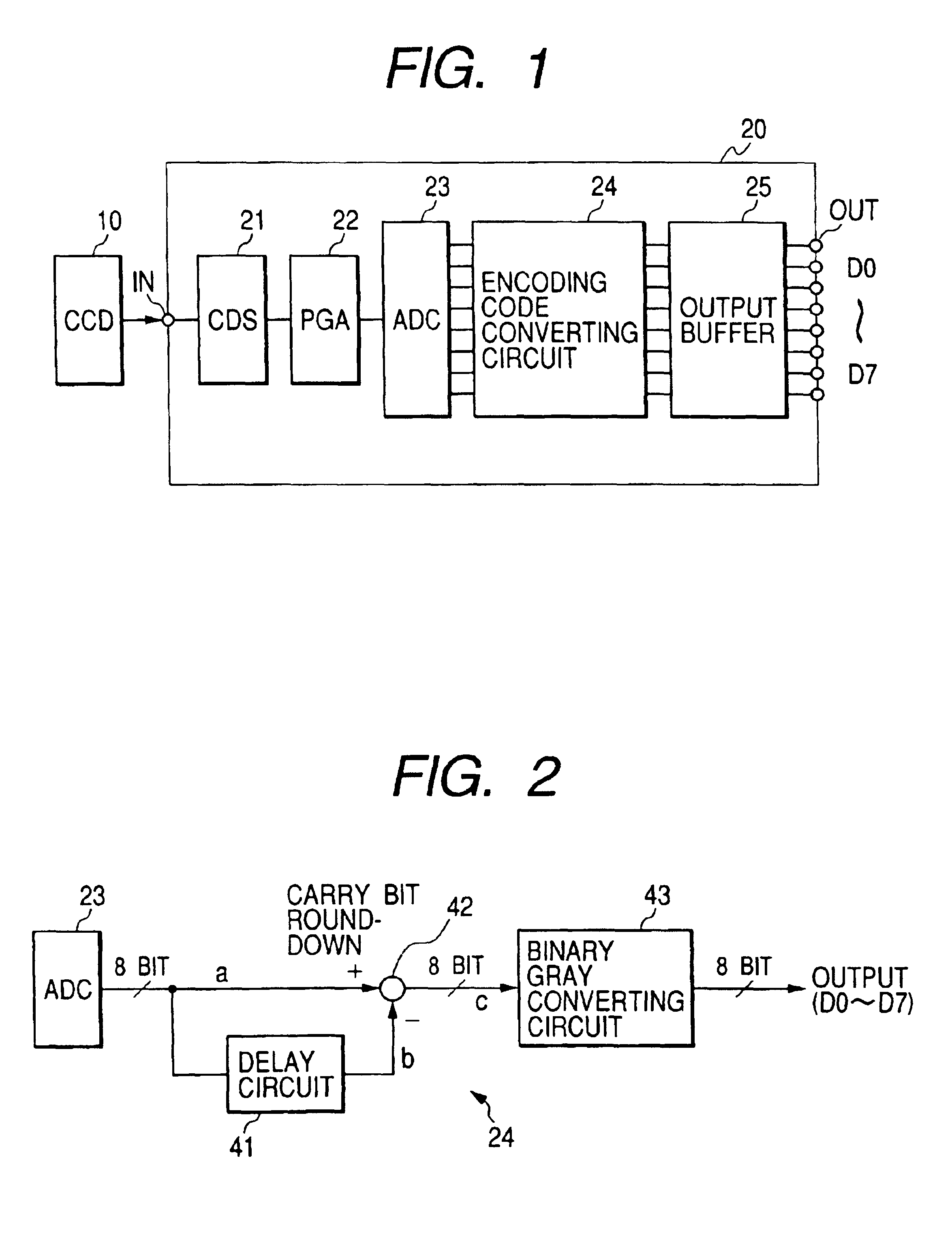
[0058]When “5” is added as the fixed value after the difference encoding from the Table 2, the binary code is changed to “100” from “101” when the decimal number changes to “−1” from “0”. Therefore, in this case, only one bit is changed over. However, in the case of this system, since the binary code changes to “000” from “111” when the decimal number changes to “3” from “2”, the number of bits to be changed over becomes 3. However, the amount of change of the signals between the adjacent pixels enters the range from “−1” to “+2” in a certain input video signal, namely in a certain imaging object (a certain video signal has a small difference of luminosity). In this case, even when the second embodiment is adapted, the number of bits to be changed when an output is changed over can be reduced and noise resulting from the change of output can also be reduced.

first embodiment

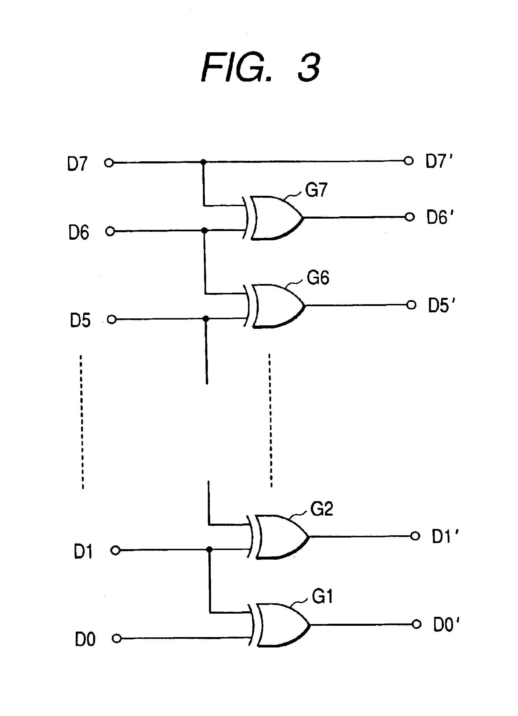
[0059]In the Table 2, the code is composed of three bits and when the number of bits increases, the range of offset binary code in which the number of bits to be changed when the output data is changed over can be reduced to 1 or less can be widened by adequately selecting the fixed value to be added. Therefore, even when the code is converted to the offset binary code after the difference encoding, the number of bits to be changed when the output digital signal is changed over can be reduced considerably, although it is not so large as in the case of the Thereby, a through-current in the output circuit can be reduced and noise resulting from change of output can also be reduced.

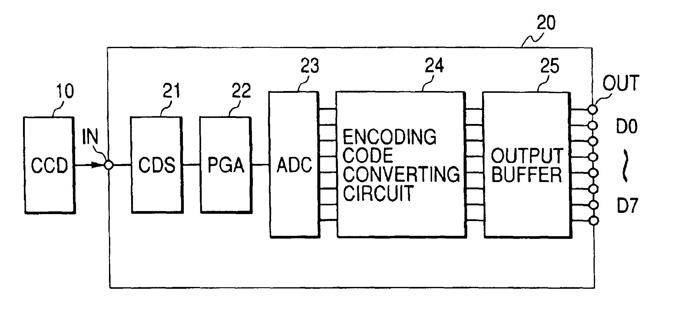
[0060]FIG. 7 shows a schematic construction of a DSP (Digital Signal Processor) 30 which executes the data process by receiving a video data outputted from the AD conversion LSI. The DSP 30 of this embodiment is composed of a gray binary difference decoding circuit 31 which receives the gray-code converted ...


PUM


Abstract

An AD-converted digital video data is encoded by a difference encoding method before it is outputted and such encoded digital video data is then outputted, after it is converted to gray code or to a predetermined code in which a fixed value is added. Problems solved include noise that is generated when the AD conversion circuit outputs video data and that migrates into a CCD side via a power supply line on a printed circuit board, and noise that appears on a display image by migration into an input terminal side from an output circuit side via the power supply line and a semiconductor substrate within an AD conversion LSI.

Description

CROSS-REFERENCE TO RELATED APPLICATION[0002]This application is a continuation of application Ser. No. 10 / 080,586 filed Feb. 25, 2002 now U.S. Pat. No. 6,781,107.BACKGROUND OF THE INVENTION[0003]The present invention relates to a noise reduction technique in an imaging system utilizing an imaging element such as a CCD (charge coupled device) and more specifically to a technique for reducing noise generated by transmission of digital image data with a code conversion system, for example a technique which can effectively be adapted to an electronic still camera (a so-called digital camera) and a video camera.[0004]As shown in FIG. 10, there is provided an imaging system such as an electronic still camera or a video camera in which an analog video signal outputted from a CCD 10 is converted into a digital signal in an LSI (large scale semiconductor integrated circuit) for AD conversion 20, this video signal is processed in a DSP (digital signal processor) 30 and the signal is then disp...

Claims


Application Information

Patent Timeline
IPC IPC(8): H01J40/00H01J40/14H03M3/00H03M7/30H04N5/335H03M7/16H04N5/357H04N5/369H04N5/372H04N5/378H04N9/07
CPCH04N5/378H04N5/335H04N5/3698H04N5/3577H04N5/357H04N25/00H04N25/617H04N25/60H04N25/709H04N25/75
Inventor AIBARA, YASUTOSHINAKAJIMA, HIROKIIMAIZUMI, EIKIMATSUURA, TATSUJI
Owner RENESAS SEMICON PACKAGE & TEST SOLUTIONS
Why Eureka
Try Eureka