
Device for driving luminescent display panel

a display panel and luminescent technology, applied in the direction of static indicating devices, identification means, instruments, etc., can solve the problems of reducing the service life of the el element, and becoming difficult to effectively apply the reverse bias voltage to the el element b

Inactive Publication Date: 2005-01-11
TOHOKU PIONEER CORP
View PDF5 Cites 36 Cited by
  • Summary
  • Abstract
  • Description
  • Claims
  • Application Information

AI Technical Summary

Benefits of technology

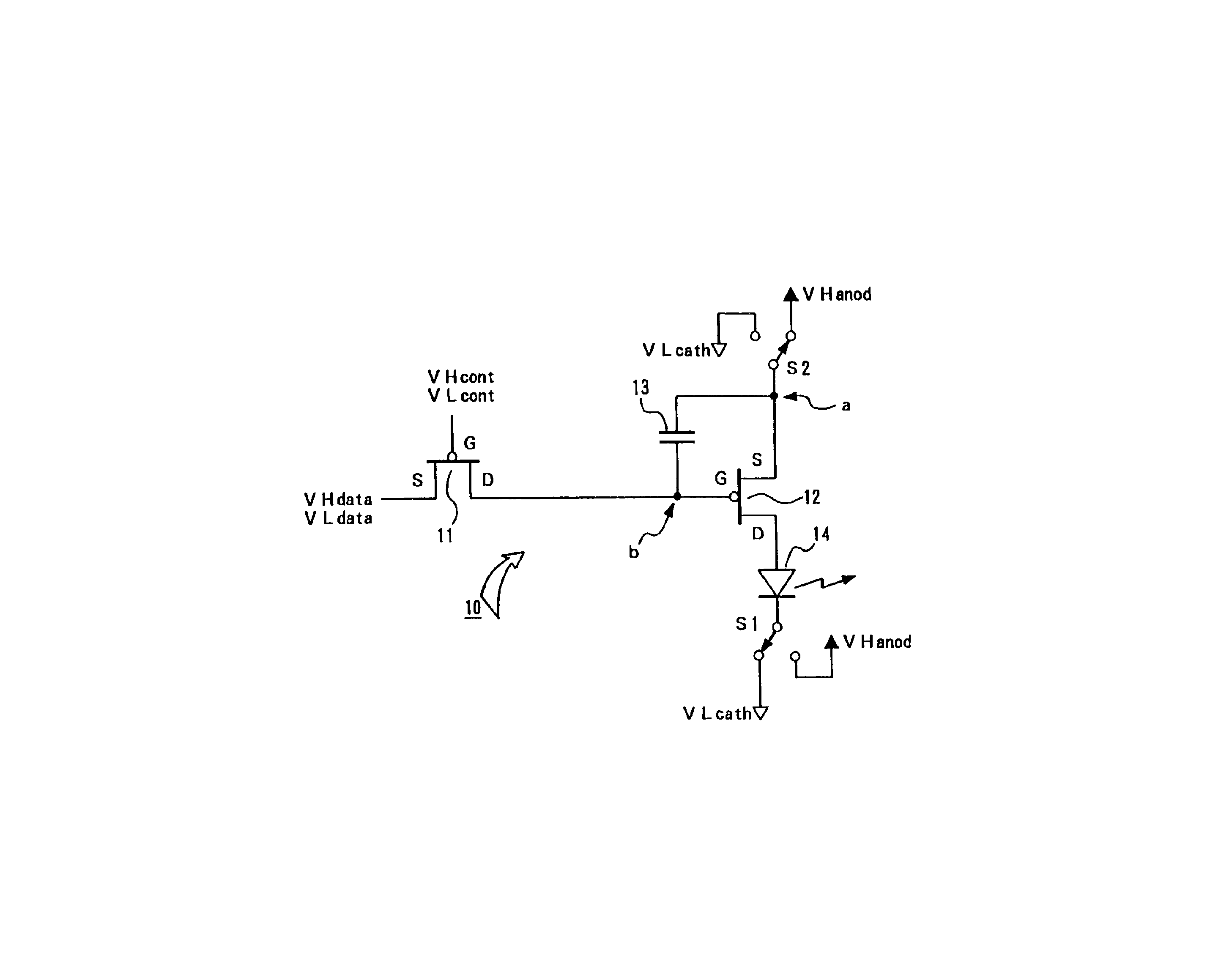
The present invention has been made in conceit of the above-described several technical points in problem and has an object to provide a device for driving a luminescent display panel, in which, in a luminescent display panel that has been constructed so that a reverse bias voltage may sequentially be supplied to the EL element, a reverse bias voltage can effectively be applied to the EL element via a drive TFT. In addition, the present invention has another object to provide a device for driving a luminescent display panel which can light-up drive by having supplied thereto a voltage level, that is relatively lower than a relevant power source circuit. Furthermore, the present invention has still another object to provide a device for driving a luminescent display panel, in which, in the circuit construction that has been exemplified in the foregoing description, it is possible to prevent the occurrence of an inconvenience that the above-described short-circuited state is brought about.

Problems solved by technology

By the way, in case where relevant control is performed by utilizing the switches S1 and S2 and, thereby, supplying each of the positive and negative power sources, by changing it over, when performing forward-directional driving and applying a reverse bias voltage, the following point in problem arises.
As a result, there occurs the phenomenon that, especially at the time when applying a reverse bias voltage, it becomes difficult to effectively apply a reverse bias voltage with respect to the EL element 14.
As a result of this, it becomes impossible to effectively apply a reverse bias voltage to the EL element 14.
Therefore, the problem remains that the effect of extending the service life of the EL element becomes halved.
Resultantly, there arises the inconvenience that short-circuiting between the VLcath and the VHdata or VLdata occurs.

Method used


Image

  • Device for driving luminescent display panel
  • Device for driving luminescent display panel
  • Device for driving luminescent display panel

Examples


second embodiment

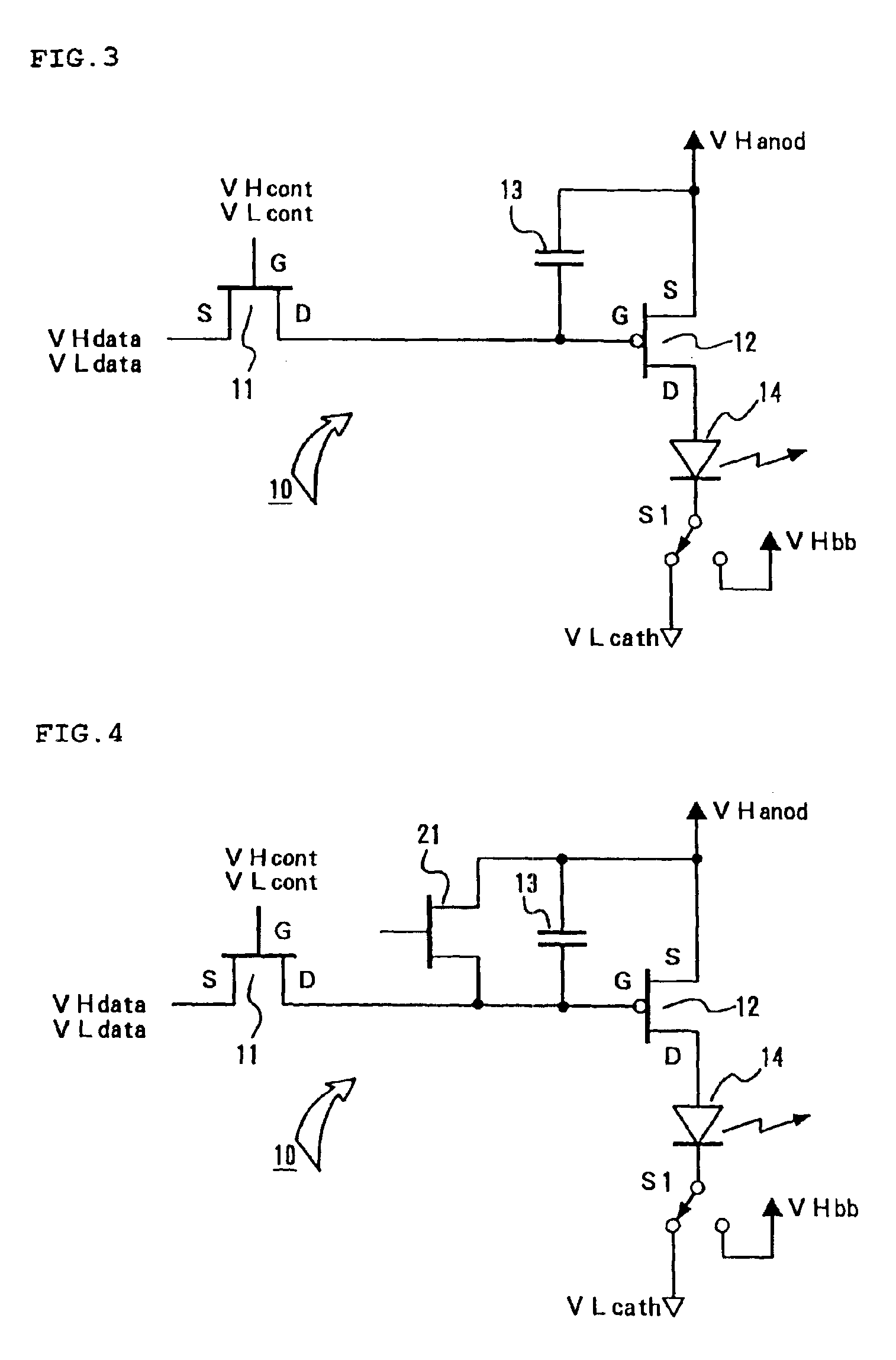
Next, FIG. 9 illustrates by a circuit construction corresponding to one pixel 10 of the present invention. In the construction, as well, illustrated in FIG. 9, as in the case of the construction illustrated in FIG. 6 which was already explained, there is also utilized the drive means, based on the use of the 3-TFT method, which realizes digital-gradation driving. Comparing it with the construction illustrated in FIG. 6, a P channel type is used as the control TFT 11. Namely, in this embodiment as well, as the drive TFT 12 and control TFT 11, a P-channel type TFT is used for each of them. Further, for an erasing TFT 21 for performing gradation expression, also, a P channel type TFT is used.

According to this construction, the operational relationship between the drive TFT 12 and the control TFT 11 is the same as in the case of the construction illustrated in FIG. 8. Namely, to the EL element 14 there can be effectively applied via the drive TFT 12 a reverse bias voltage in this state ...

third embodiment

FIG. 10 illustrates by a circuit construction corresponding to one pixel 10 of the present invention. The construction illustrated in FIG. 10 is formed into a type wherein, in addition to the construction illustrated in FIG. 9, there is equipped a diode 18 that is connected in parallel to the drive TFT 12 and, when applied with a reverse bias voltage, becomes electrically conductive. In this construction as well, when applying a reverse bias voltage to the EL element 14, the changeover switches S1 and S2 are each changed over to the opposite state to that illustrated. The diode 18 that has been connected in parallel to the drive TFT 12 becomes electrically conductive and this enables effectively applying a reverse bias voltage to the EL element 14.

And, in a state where the EL element 14 is applied with a reverse bias voltage, since each of the TFT 21 and TFT 11 is constructed using a P channel type transistor, it is maintained in an “off” state. Accordingly, as was explained in FIG....

fourth embodiment

FIG. 11 illustrates the present invention by a circuit construction corresponding to one pixel 10. This construction illustrated in FIG. 11 utilizes drive means for driving with the use of a so-called “current mirror” method. The construction is made so that the writing processing into the capacitor for holding electric charge as well as the light-up driving operation may be performed through the performance of the current mirror operation. In this construction illustrated in FIG. 11, also, a power source voltage of VHanod=10 V and a power source voltage of VHcath=−5 V may be utilized. Namely, in case where causing a forward-directional electric current to flow into the EL element 14 and in case where applying a reverse bias voltage to the EL element 14, it is arranged that each of the VHanod=10 V and the VLcath=−5 V be used by having its output level inverted in terms of the polarity via the changeover switch S1 or S2.

Also, a TFT 22 that is of a P-channel type is symmetrically equi...


PUM


Abstract

Provided is a device for driving an active matrix type luminescent display panel, which can effectively apply a reverse bias voltage to a luminescent element via a drive TFT. A luminescent element 14 constituting one pixel 10 is light-up driven by a control TFT 11 and a drive TFT 12. A serial circuit of the drive TFT 12 and the luminescent element 14 is connected to a power source circuit via a switch S1 and a switch S2, whereby a state where a forward-directional current is supplied to the luminescent element or a state where a reverse bias voltage is applied to the luminescent element is selected. By using, as the control TFT 11 and the drive TFT 12, TFT of the channel type of that is the same, it is possible to maintain the drive TFT 12 to be in an “on” state when having applied a reverse bias voltage to the luminescent element 14. By doing so, it becomes possible to effectively apply a reverse bias voltage to the luminescent element.

Description

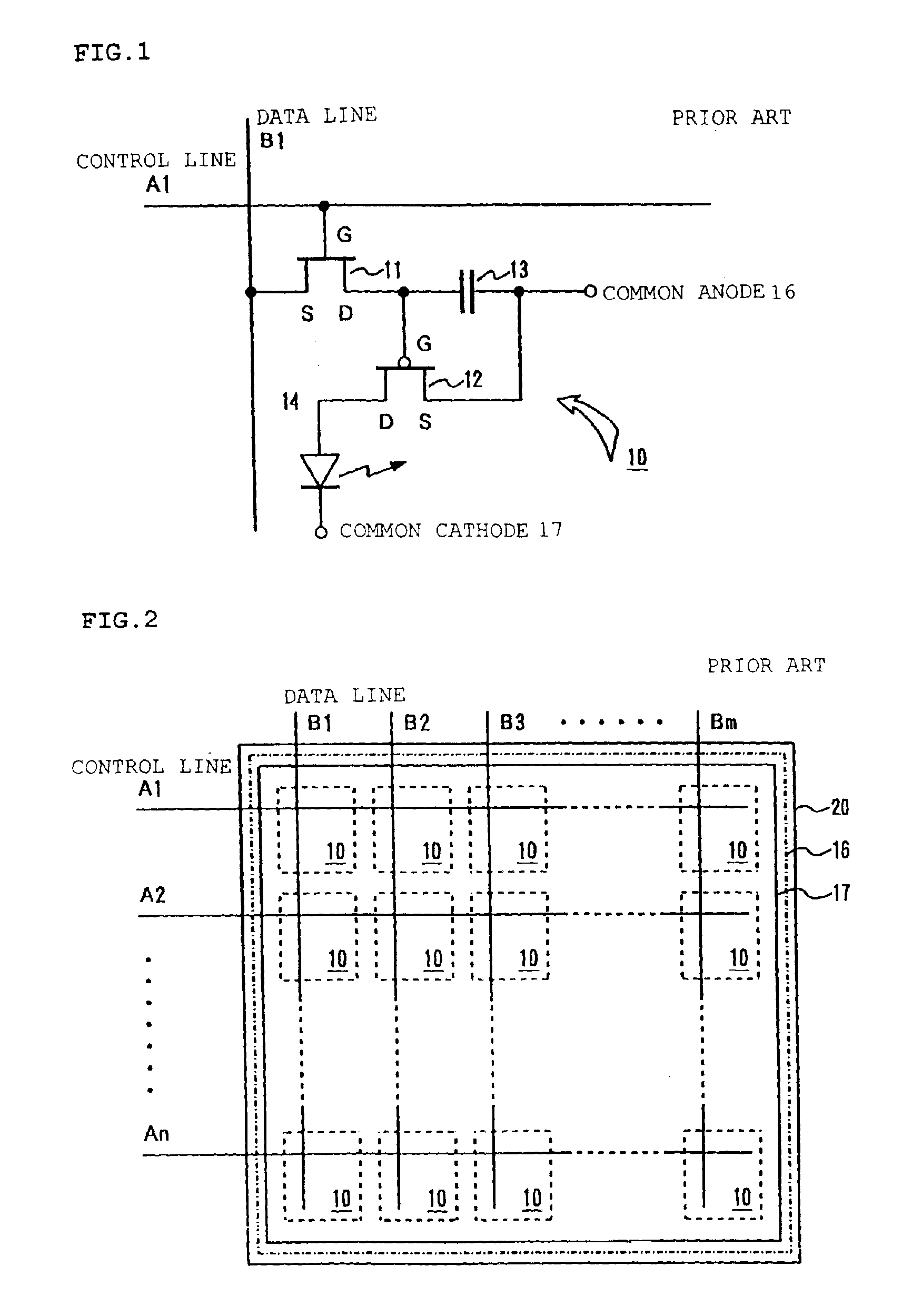
BACKGROUND OF THE INVENTION1. Field of the InventionThe present invention relates to a device for driving a display panel that performs active driving of a luminescent element constituting a pixel by, for example, a TFT (Thin Film Transistor) and, more particularly, to a device for driving a display panel, which enable effectively applying a reverse bias voltage with respect to the luminescent element via a driving TFT.2. Description of the Related ArtDevelopment of a display that uses a display panel constructed of luminescent elements arranged in the form of a matrix has gone on being widely made. As a luminescent element that is used in such display panel, attention has been drawn toward an organic EL (electroluminescence) element wherein organic material is used in the luminescent layer. One of the reasons therefor is that, by using in a luminescent layer of the EL element an organic compound from which good luminescent property can be expected, the increase in the efficiency an...

Claims


Application Information

Patent Timeline
IPC IPC(8): G09G3/32H01L51/50G09F9/30G09G3/20G09G3/30H01L27/32
CPCG09G3/3233G09G2300/0809G09G2300/0842G09G2300/0852G09G2320/043G09G2300/0866G09G2310/0254G09G2310/0256G09G2300/0861G09G3/30
Inventor YOSHIDA, TAKAYOSHI
Owner TOHOKU PIONEER CORP
Learn More