Apparatus for testing reliability of interconnection in integrated circuit

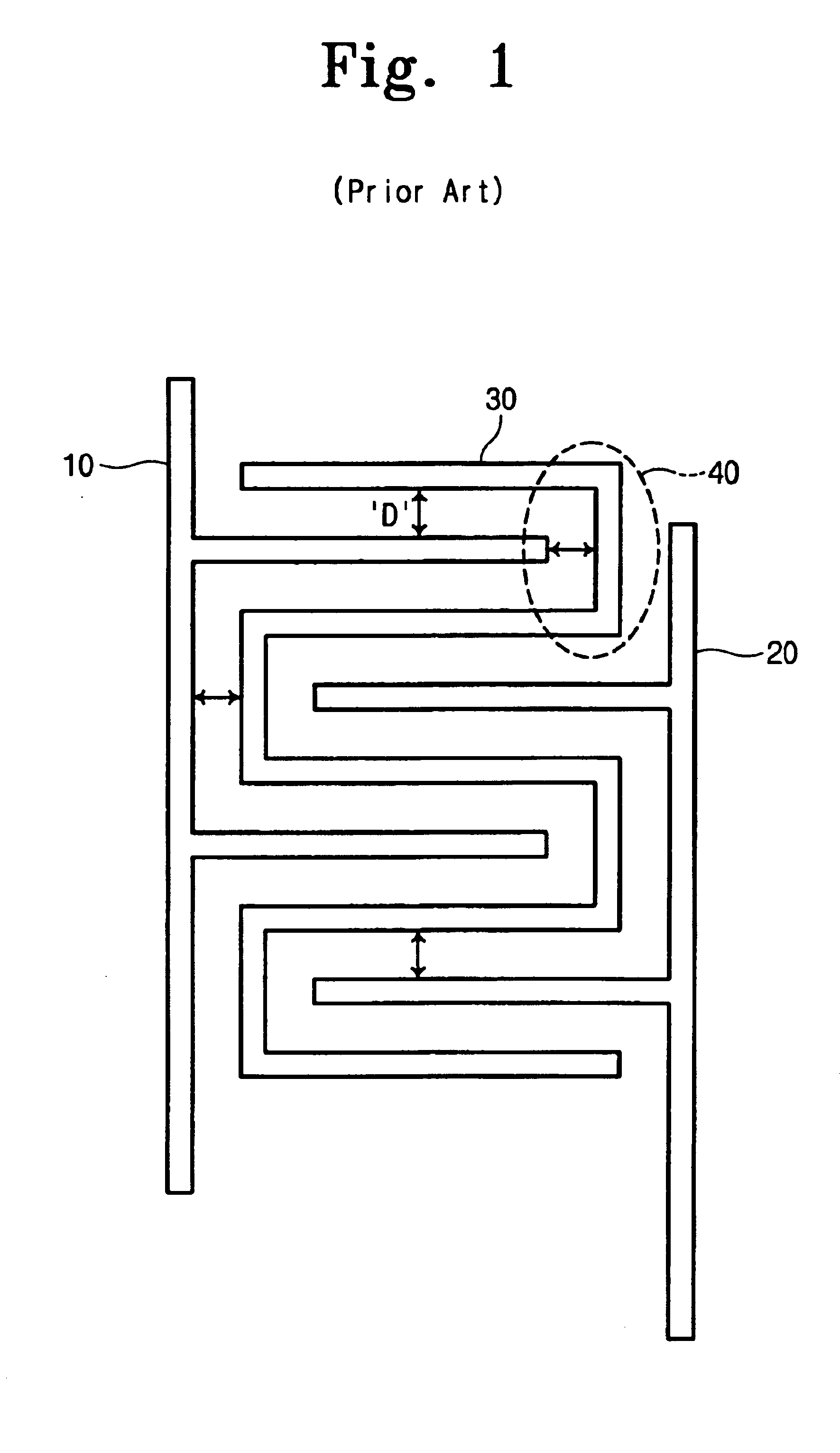
a technology of interconnection and apparatus, applied in the direction of electronic circuit testing, measurement devices, instruments, etc., can solve the problems of inability to connect cells through contact formed between interconnection and interlayer dielectric layer, and inability to detect real-world problems too simplistically and effectively. , to achieve the effect of easily and effectively detecting a problem spo

Inactive Publication Date: 2005-01-11
SAMSUNG ELECTRONICS CO LTD
View PDF4 Cites 21 Cited by
  • Summary
  • Abstract
  • Description
  • Claims
  • Application Information

AI Technical Summary

Benefits of technology

It is another object of the present invention to provide a test apparatus which may easily and effectively detect a problem spot of a leakage or a short between vias and interconnections in multilayered interconnections.
It is stil

Problems solved by technology

In a very narrow region of a highly integrated semiconductor device, it is very difficult to connect cells through a contact formed between an interconnection and an interlayer dielectric layer.
This produces undesirable shorts between circuit nodes that should not be connected or opens between circuit notes that should be connected.
However, such a method evaluates leakage protection reliability only between interconnections in one layer.
The form works for testing the reliability of an interlayer dielectric layer, but is too simplistic to detect real world problems related to a via or a contact according to multilayered interconnections of a semiconductor device.
However, in a highly integrated semiconductor device, a small difference in process conditions may produce a large difference in results or effects.
But, when the copper is processed, the processed surface of copper or copper oxide tends to be rough.
Thus, the use of copper may produce a narrow interconnecti

Method used


Image

  • Apparatus for testing reliability of interconnection in integrated circuit
  • Apparatus for testing reliability of interconnection in integrated circuit
  • Apparatus for testing reliability of interconnection in integrated circuit

Examples


embodiment 1

FIG. 3 illustrates a partial top plan view of a part in an embodiment where a comb pattern and a serpentine pattern are provided according to a first structure of the present invention.

FIG. 4 illustrates a partial perspective view of parts which will be repeatedly formed, in an embodiment having the same partial plan view with FIG. 3, i.e., a tooth portion 120 and a connected length portion 110 of a comb pattern 100, and a neighboring unit part 340 and a connection part 350 of a serpentine pattern.

Referring to FIGS. 3 and 4, in the present embodiment 1, the tooth portion 120 of the comb pattern 100 is located at the central position between vias 330 formed at the ends of tooth parallel parts 310 of the serpentine pattern. The vias 330 extend to an upward direction from the ends of the tooth parallel parts 310, respectively, and the tooth parallel parts 310 are laterally spaced from the tooth portion 120 by a minimum design length ‘D’ according to a design rule in a semiconductor dev...

embodiment 2

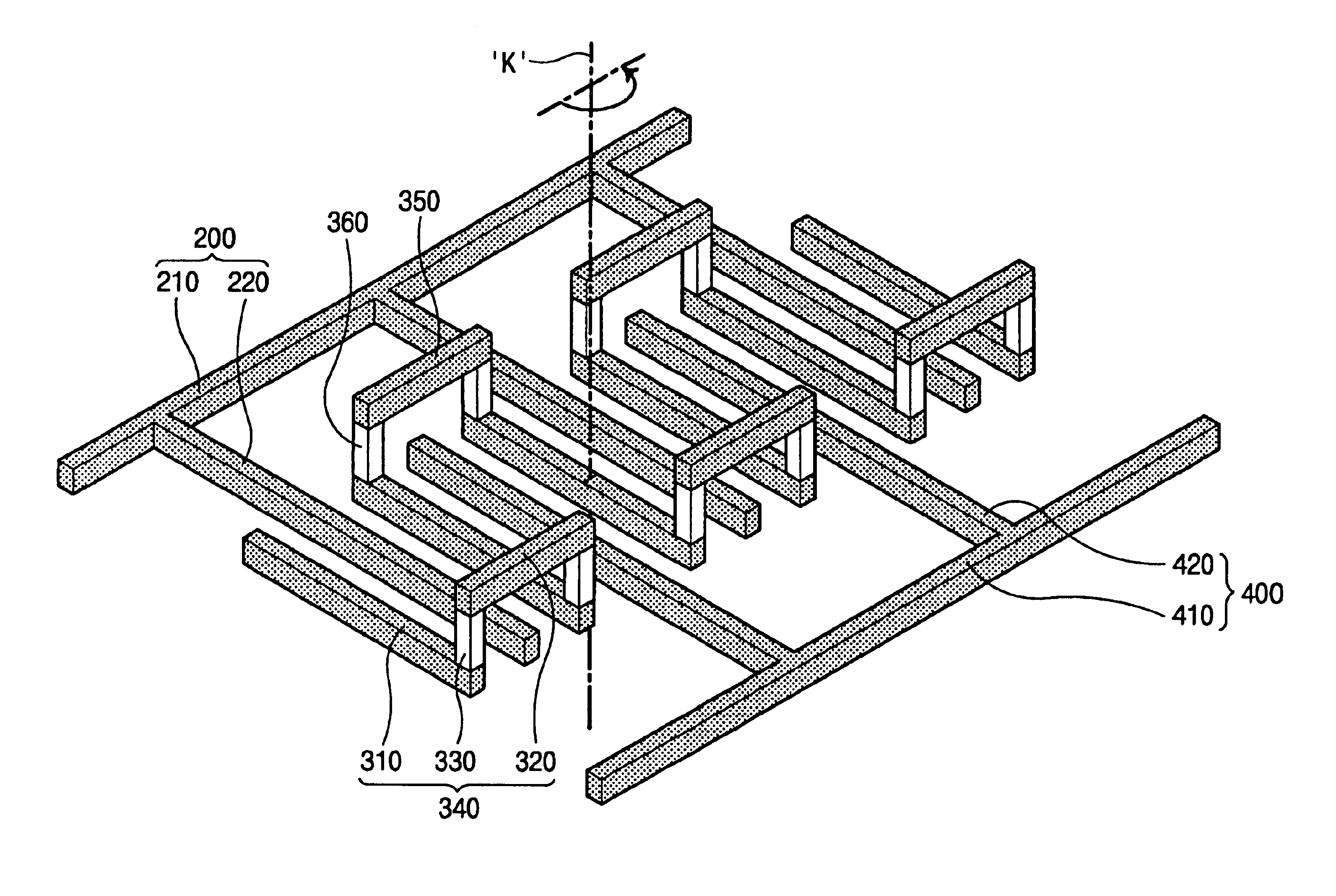
FIG. 8 illustrates a partial top plan view showing a part in a second embodiment, in which two comb patterns 200 and 400 and one serpentine pattern 300 are provided according to a second structure. In the present embodiment, one comb pattern 400 is further placed laterally from the serpentine pattern at the opposite position of the original comb pattern 200. The serpentine pattern 300 also acts as forming an electric field with respect to the additional comb pattern 400.

FIG. 9 illustrates a partial isometric view showing parts which will be repeatedly formed, in an embodiment having the same partial plan of FIG. 8.

Referring to FIGS. 8 and 9, the length portions 210 and 410, and the tooth portions 220 and 420 of the two comb patterns 200 and 400, and the tooth parallel part 310 of the serpentine pattern 300 are formed at a lower interconnection layer under an interlayer dielectric layer. The connection part 350 and the length parallel part 320 of the serpentine pattern 300 are formed...


PUM


Abstract

In the present invention, an apparatus of testing a leakage protection reliability of an integrated circuit interconnection. The apparatus has at least one comb-like pattern, a serpentine-like pattern and means of applying a bias to the patterns and forms a maximum field region at an interconnection formed around a via, i.e., at the end of a tooth portion composing the comb-like pattern. In one structure of the present invention, the comb-like pattern is formed at one level, and the serpentine-like pattern has a plurality of unit parts corresponding to the tooth portions, respectively, and connection parts connecting the neighboring two unit parts. Each of the unit parts is formed at the same level with the comb-like pattern and spaced apart from the tooth portion by a minimum design length according to a design rule. The unit part has vias formed through an interlayer dielectric layer at the both ends of a tooth parallel part, two tooth parallel parts connected with the vias, respectively, and a length parallel part electrically connecting two tooth parallel parts.

Description

FIELD OF THE INVENTIONThe present invention relates to an apparatus of testing an integrated circuit interconnection. More particularly, the present invention relates to a test apparatus which is suitable for testing the leakage protection reliability of an integrated circuit interconnection having a high via density.BACKGROUND OF THE INVENTIONAs semiconductor devices become highly integrated, the sizes of individual devices and wires or interconnections become smaller. As one method of highly integrating the semiconductor devices, semiconductor devices may be made to have three-dimensional structures. For example, interconnections of connecting semiconductor devices are formed of a plurality of layers to have a three-dimensional structure in the semiconductor devices.In a very narrow region of a highly integrated semiconductor device, it is very difficult to connect cells through a contact formed between an interconnection and an interlayer dielectric layer. For example, in a plura...

Claims


Application Information

Patent Timeline
IPC IPC(8): G01R31/28G01R31/02
CPCG01R31/2853
Inventor SONG, WON-SANGKIM, JUNG-WOOLEE, CHANG-SUBKIM, SAM-YOUNGWEE, YOUNG-JINPARK, KI-CHUL
Owner SAMSUNG ELECTRONICS CO LTD
Why Eureka
Try Eureka