Laser apparatus, laser irradiation method, manufacturing method for a semiconductor device, semiconductor device and electronic equipment

a laser irradiation and laser irradiation technology, applied in metal working equipment, manufacturing tools, welding/soldering/cutting articles, etc., can solve the problems of loss of time according to direction change, difficult inability to uniformly treat the substrate, etc., to achieve the effect of improving processing efficiency

Inactive Publication Date: 2005-01-18
SEMICON ENERGY LAB CO LTD
View PDF8 Cites 38 Cited by
  • Summary
  • Abstract
  • Description
  • Claims
  • Application Information

AI Technical Summary

Benefits of technology

The present invention has been made in view of the above problems, and therefore it is an object of the present invention to provide a continuous oscillation laser apparatus and a m

Problems solved by technology

Therefore, it is impossible to uniformly treat the substrate.
However, there is a loss of time according to the direction change that is a problem in moving the substrate.
At this time, when the moving speed of the irradiation position is changed depending on the position of the substrate, it is difficult to uniformly treat the substrate.
Consequently, it necessarily takes a predetermined time to change the direction of the substrate,

Method used


Image

  • Laser apparatus, laser irradiation method, manufacturing method for a semiconductor device, semiconductor device and electronic equipment
  • Laser apparatus, laser irradiation method, manufacturing method for a semiconductor device, semiconductor device and electronic equipment
  • Laser apparatus, laser irradiation method, manufacturing method for a semiconductor device, semiconductor device and electronic equipment

Examples


embodiment 1

(Embodiment 1)

In this embodiment, a description will be made of a case where the object to be processed is irradiated with the laser light twice or more by moving the stage on a rotating body where the object to be processed is set up in one direction and thereafter moving it in the reverse direction.

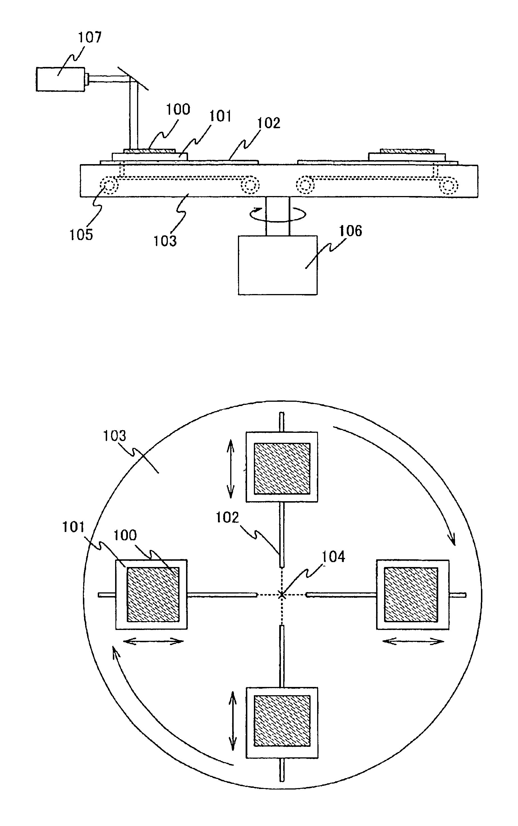
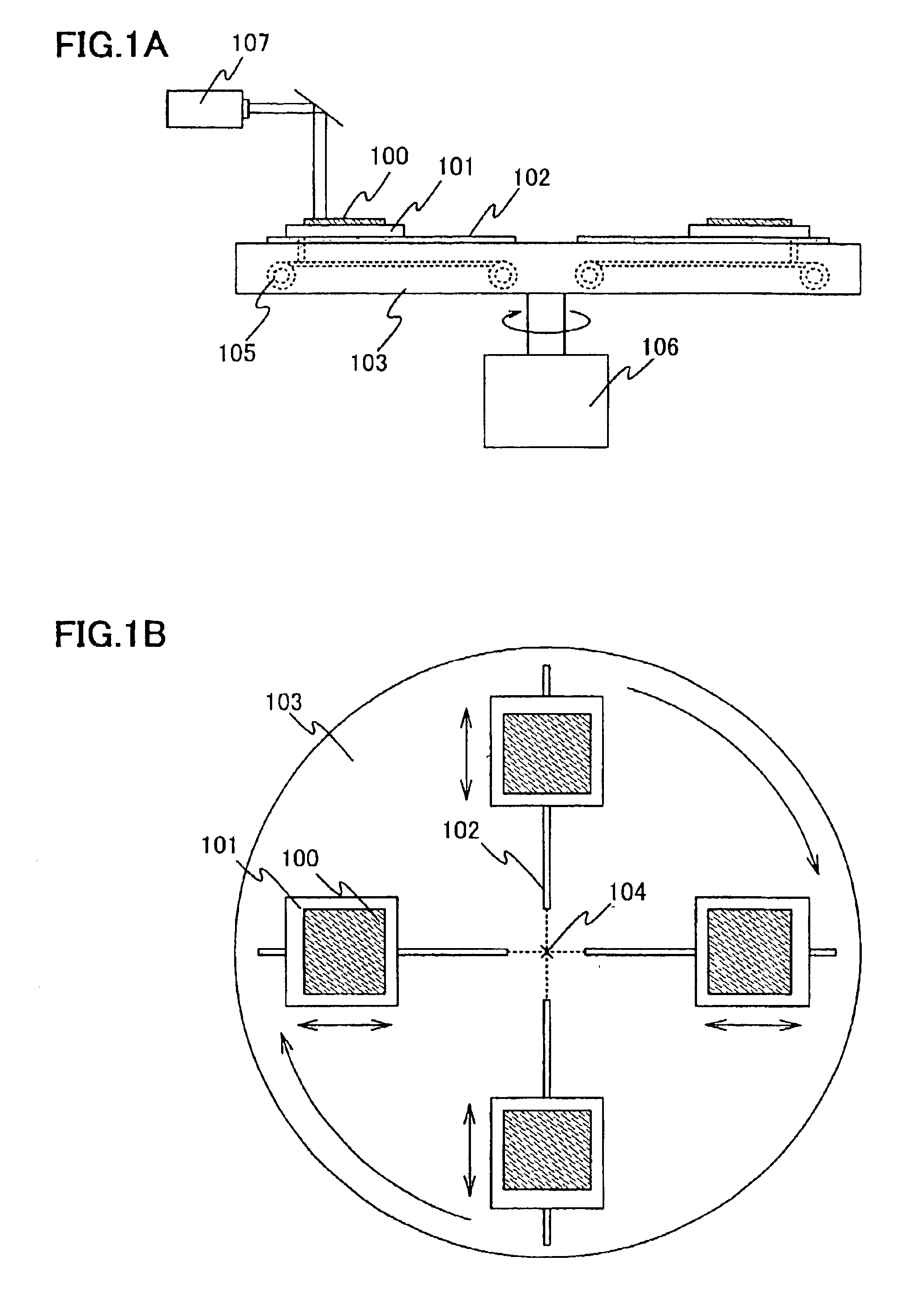
FIG. 4A shows a top view of a rotating body and a stage which the laser apparatus of this embodiment comprise. In this embodiment, the laser apparatus capable of treating six objects to be processed at the same time will be described. Incidentally, the number of objects to be processed can be arbitrarily determined by a designer.

The laser apparatus of the present invention shown in FIG. 4A has six stages 201 corresponding to first means for setting up the object to be processed thereon. It is possible to further enhance the processing efficiency by providing a plurality of stages and treating a plurality of objects to be processed at the same time. On each of the stages 201, an object t...

embodiment 2

(Embodiment 2)

In this embodiment, in the case where laser irradiation is performed a plurality of times, a case is described where the laser light is irradiated so that the edge portions of the laser light in each irradiation do not overlap with each other.

In general, in the laser light, an energy of the edge portion is smaller than the other portion. Therefore, in this embodiment, several laser irradiations are carried so that the edge portions of the laser light should not overlapped with each other, and thereby in order that the smaller energy of edge portion is covered.

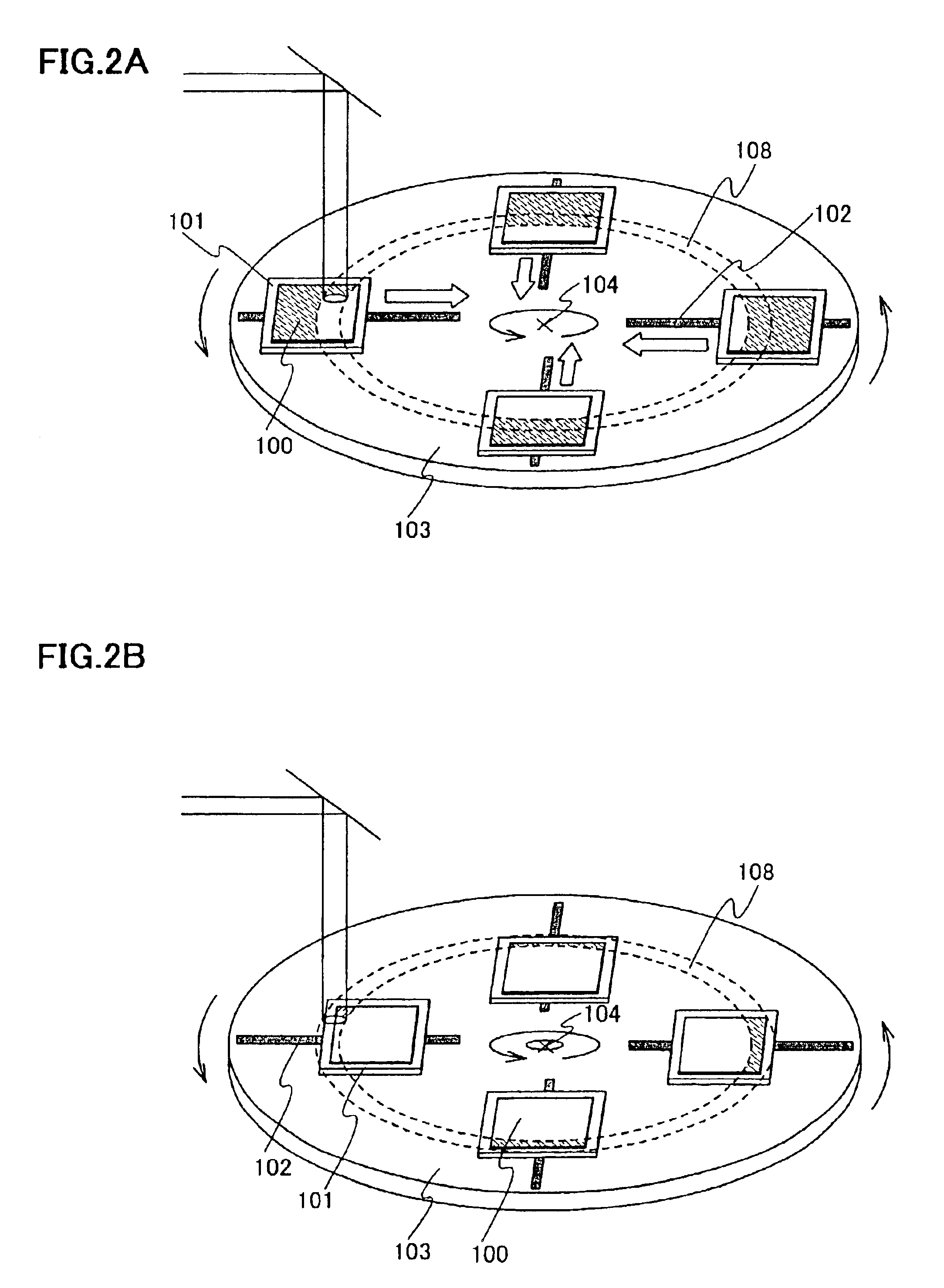
In order to prevent the edge portions of the laser light in each irradiation from overlapping with each other, there is a method in which a range where the stage is moved is shifted in the first laser irradiation and the second laser irradiation. FIG. 5A is a sectional view of the laser apparatus in the first laser irradiation and FIG. 5B is a sectional view of the laser apparatus in the second laser irradiation. ...

embodiment 3

(Embodiment 3)

In this embodiment, in the case where laser irradiation is performed a plurality of times, a method is described in which the laser light is irradiated so that the edge portions of the laser light in each irradiation do not overlap with each other, and which is different from the method of Embodiment 2.

In this embodiment, in order for the edge portions not to overlap, in the first laser irradiation and the second laser irradiation, the irradiation position of the laser light on the rotating body is changed. FIG. 6 shows a locus of the laser light in the first laser irradiation and the second laser irradiation on the rotating body. Reference numeral 401 shows a rotating body and 402 shows an object to be processed.

Reference numeral 403 shows a locus of the laser light in the first irradiation and 404 shows a locus of the laser light in the second laser irradiation. The locus 403 of the laser light and the locus 404 of the laser light overlap with each other and the edge...


PUM


Abstract

To provide a continuous oscillation laser apparatus, and a manufacturing method of a semiconductor device using the continuous oscillation laser apparatus, which can enhance processing efficiency. A laser apparatus according to the present invention includes: a laser oscillation apparatus; a unit for rotating an object to be processed; a unit for moving the object to be processed toward a center of the rotation or toward an outside from the center; and an optical system for processing a laser light outputted from the laser oscillation apparatus and irradiating the processed laser light to a definite region in a moving range of the object to be processed, in which, while the object to be processed is rotated, the object to be processed is moved toward the center of the rotation or toward the outside from the center to move a position where the definite region and the object to be processed overlap.

Description

BACKGROUND OF THE INVENTION1. Field of the InventionThe present invention relates to a laser processing apparatus and a laser irradiation method for crystallizing a semiconductor substrate, a semiconductor film or the like using a laser light or for performing activation after ion implantation, a semiconductor device formed by using the laser apparatus and a manufacturing method therefor, and an electronic equipment using the semiconductor device.2. Description of the Related ArtIn recent years, a technique of forming a TFT on a substrate has greatly progressed, and its application and development for active matrix semiconductor display device has been advanced. In particular, since a TFT using a polysilicon film has higher field-effect mobility than a TFT using a conventional amorphous silicon film, it enables high speed operation. Therefore, although the pixel is conventionally controlled on a driving circuit provided outside the substrate, it is possible to control the pixel on t...

Claims


Application Information

Patent Timeline
IPC IPC(8): B23K26/08
CPCB23K26/0823B23K2201/36B23K2101/36
Inventor YAMAZAKI, SHUNPEITANAKA, KOICHIROMIYAIRI, HIDEKAZUSHIGA, AIKOSHIMOMURA, AKIHISA
Owner SEMICON ENERGY LAB CO LTD
Why Eureka
Try Eureka