Surface-mount package for an optical sensing device and method of manufacture

Inactive Publication Date: 2005-01-18
XENOGENIC DEV LLC
View PDF5 Cites 52 Cited by
  • Summary
  • Abstract
  • Description
  • Claims
  • Application Information

AI Technical Summary

Benefits of technology

As described above, a plurality of the packages can be simultaneously fabricated by defining a plurality of chip carriers in a chip carrier wafer, preferably formed of an LTCC material, and defining a plurality of capping chips in a capping chip wafer. After placement of the device chips on the chip carriers of the chip carrier wafer, the carrier and capping wafers can be bonded together before singulation to form the individual packages. As such, an optical sensor package of this invention has the ability to be array tested with other packages f

Problems solved by technology

A drawback of this type of packaging approach is that each sensing chip and package must be individually handled and tested, and the packages are not suitable for

Method used


Image

  • Surface-mount package for an optical sensing device and method of manufacture
  • Surface-mount package for an optical sensing device and method of manufacture

Examples


Embodiment Construction

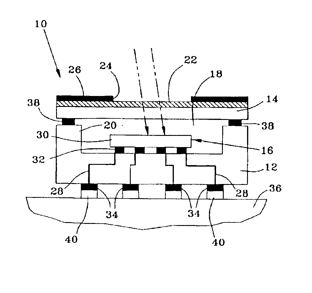
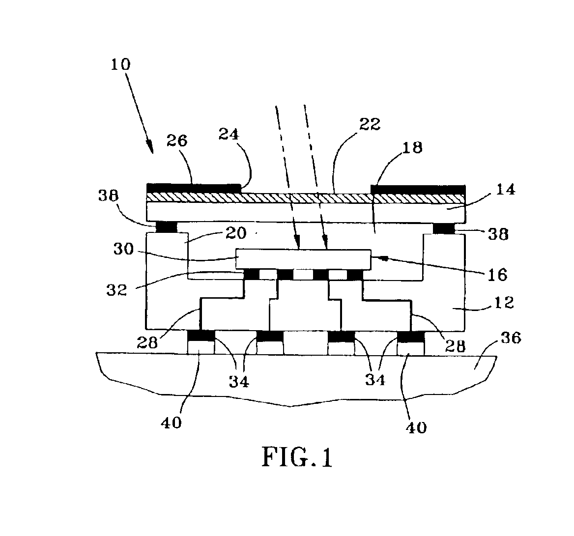
FIG. 1 represents an optical sensor package 10 that can be fabricated and surface mounted in accordance with this invention. The package 10 is shown as being formed by solder bonding a device chip carrier 12 to a capping chip 14, such that an optical sensing device chip 16 is enclosed and protected within a cavity 18 defined by and between the capping chip 14 and the device chip carrier 12, e.g., the cavity 18 is formed by a recess 20 in the device chip carrier 12. While shown as being a stack of an individual capping chip 14 and chip carrier 12, the invention preferably entails the use of wafers that are bonded together and later singulated to form any desired number of packages 10 of the type shown in FIG. 1. With this approach, a device chip carrier wafer is processed to have an array of recesses 20, each of which will form a cavity 18 with a capping wafer to contain an optical sensing device chip 16.

The capping chip 14 is preferably silicon, more preferably monocrystallographic ...


PUM


Abstract

An optical sensor package capable of being surface mounted, and in a form that enables multiple packages to be fabricated simultaneously and then array tested in a wafer stack prior to singulation. The package comprises a chip carrier, a device chip electrically and mechanically connected to a first surface of the chip carrier with solder connections, and a capping chip secured to the chip carrier to hermetically enclose the device chip. The device chip has an optical sensing element on a surface thereof, while the capping chip has means for enabling radiation to pass therethrough to the device chip. The chip carrier includes conductive vias that are electrically connected to the solder connections of the device chip and extend through the chip carrier to bond pads on a second surface of the chip carrier, enabling the package to be surface mounted with solder connections to a suitable substrate.

Description

BACKGROUND OF INVENTION1. Field of the InventionThe present invention generally relates to packaging of optical sensors. More particularly, this invention relates to a package containing an optical sensing chip and capable of being surface mounted to a circuit board to provide electrical connection between the sensing chip and conductors on the circuit board.2. Description of the Related ArtA variety of optical sensors are known that employ a radiation-sensing element, such as a thermopile, fabricated in or on the surface of a silicon chip (referred to herein as a sensing chip). The sensing chip is often placed within a protective package, such as a TO-x type can, with a window that allows radiation to reach the sensing element. The sensing chip is then wirebonded to electrically connect the sensing element to bond pads on the package, which in turn must then be mounted to a circuit board in a manner that electrically and physically interconnects the sensing element to the board cir...

Claims


Application Information

Patent Timeline
IPC IPC(8): G01J5/00H01L23/02H01L23/10H01L25/16
CPCH01L23/10H01L25/167H01L2224/16H01L2924/09701H01L2924/15153H01L2924/15165H01L2924/10253H01L2924/15174H01L2924/16195H01L2924/00
Inventor LOGSDON, JAMES H.CHAVAN, ABHIJEET V.BORZABADI, HAMID R.
Owner XENOGENIC DEV LLC
Why Eureka
Try Eureka