
Semiconductor device and method of relaxing thermal stress

a technology of a semiconductor and a relaxation device, which is applied in the direction of semiconductor devices, semiconductor/solid-state device details, electrical equipment, etc., can solve the problems of thermal breakdown, material heat dissipation performance as substrates is inferior, and section largely affects the reliability and life of the entire power semiconductor modul

Inactive Publication Date: 2005-01-18
FUJI ELECTRIC CO LTD
View PDF12 Cites 52 Cited by
  • Summary
  • Abstract
  • Description
  • Claims
  • Application Information

AI Technical Summary

Benefits of technology

According to the present invention, the insulating substrate has means for relaxing thermal stress concentration created in the solder due to thermal cycling.

Problems solved by technology

Therefore, the fatigue life of the soldered section largely affects the reliability and the life of the entire power semiconductor module.
This interrupts heat dissipation from the silicon chip 3, raising the junction temperature of the semiconductor element, which will lead to possible thermal breakdown.
Thus, the materials have inferior heat dissipation performance as substrates.
Furthermore, these materials with low thermal expansion, being manufactured by using such a special method as to sinter or impregnate SiC or Mo having a high melting point and being hard to be machined, are expensive compared with copper material.
This increases the cost of the semiconductor module.
Although this method is effective for extending the life of the soldered section, however, the thermal resistance at the joined section increases with the increasing thickness, lowering the heat dissipation.
Furthermore, increasing the thickness of the soldered section increases the amount of solder being used to produce solder balls or cause a solder overflow in a module assembling process (a soldering process), lowering the product yield.
Further, it is technically difficult to uniformly maintain the thickness of the solder layer.

Method used


Image

  • Semiconductor device and method of relaxing thermal stress
  • Semiconductor device and method of relaxing thermal stress
  • Semiconductor device and method of relaxing thermal stress

Examples


Embodiment Construction

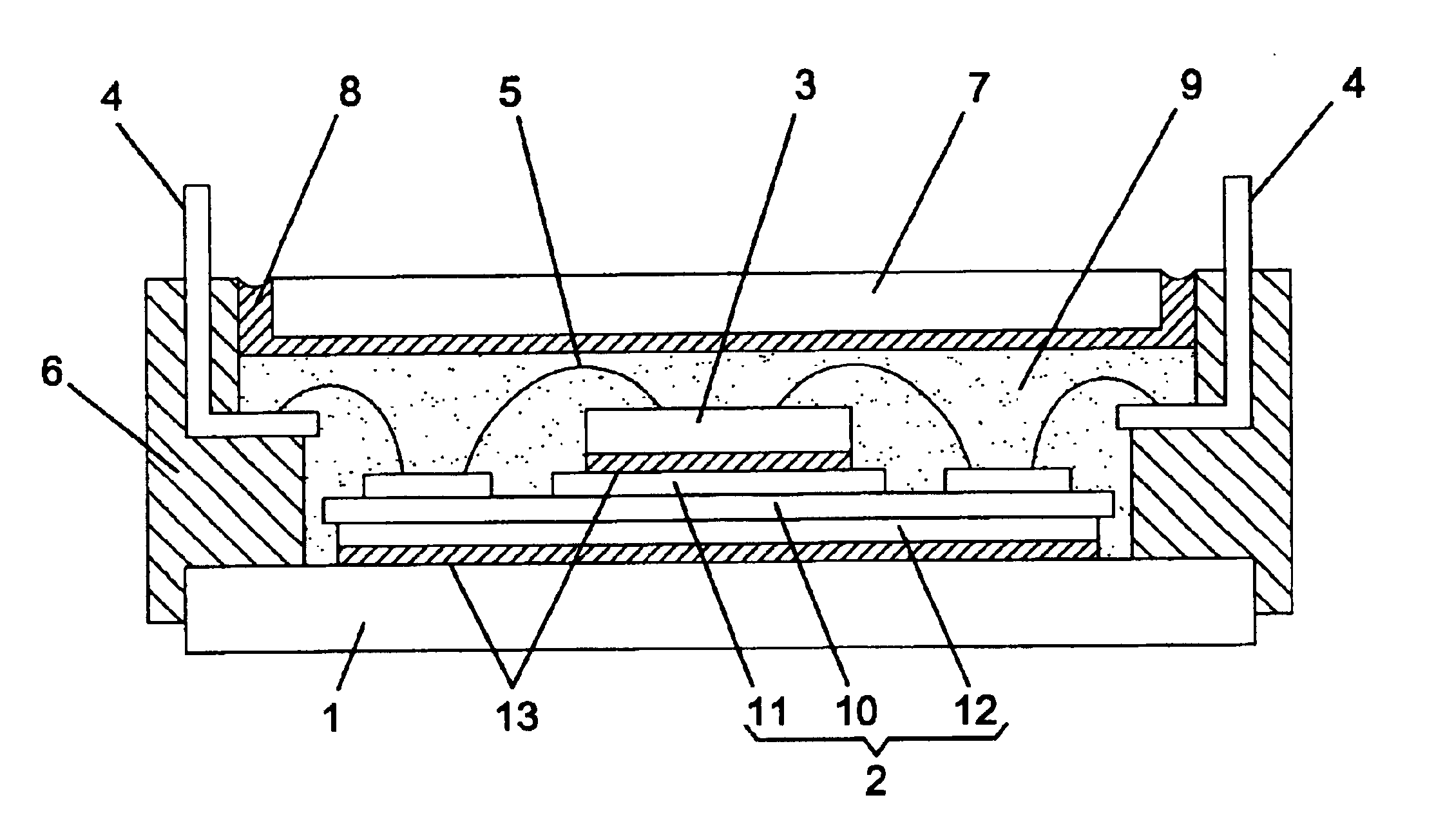
In the drawings, components corresponding to those shown in FIG. 11 are denoted with the same reference numerals. The insulation substrate 2 according to the present invention includes means for relaxing thermal stress applied to soldered sections. The following embodiments disclose the means for relaxing thermal stress.

Referring to FIGS. 1A to 1C, which show a first embodiment according to the present invention, the insulation substrate 2 comprises a square ceramic substrate 10 with bonding conductor patterns 11 and 12 formed on the top and bottom surfaces of the ceramic substrate 10. The bonding is carried out by a direct bonding method or an active metal bonding method. Here, the ceramic substrate 10 can be made of a composite material of aluminum oxide with zirconium oxide added thereto, such as described in Japanese Patent Nos. 2,883,787 and 3,176,815. The size thereof, for example, can be 0.25 mm in plate thickness and 40 mm by 40 mm in outer dimensions. Each of the conductor ...


PUM

PropertyMeasurementUnit
distanceaaaaaaaaaa
widthaaaaaaaaaa
thicknessaaaaaaaaaa

Abstract

A semiconductor device has an insulating substrate with conductor patterns bonded to and formed on both the top and bottom surfaces of a ceramic substrate. Soldering is provided between the conductor pattern on the top surface side and a heat developing chip component such as a power semiconductor element is mounted thereon. Between the conductor pattern on the bottom surface side and a heat dissipating metal base plate, each of four corners of the ceramic substrate is chamfered to form a chamfered section with a chamfered dimension of 2 to 10 mm. Alternatively, slits can be formed at the four corners on the bottom surface side. Moreover, the thickness of the conductor patterns can be controlled in relation to the ceramic substrate. These configurations relax the stress concentration created in the soldered section due to a thermal cycle.

Description

BACKGROUNDAn assembled power semiconductor module is shown in FIGS. 10 and 11, where reference numeral 1 denotes a metal base (for example, a copper plate) for heat dissipation, numeral 2 denotes an insulating substrate mounted on the metal base 1, and numeral 3 denotes a heat developing chip component such as a power semiconductor element (hereinafter referred to as “a silicon chip”), which is mounted on an upper surface of the insulating substrate 2. The metal base 1 can be a plate-like metal or a metal provided with a heat radiation fin. When the plate-like metal is used, the heat radiation fin can be joined thereto.The power semiconductor element is referred to as an IGBT or FWD (Free Wheeling Diode). Reference numeral 4 denotes an external terminal for a main circuit formed in the above power semiconductor element and associated components, numeral 5 denotes a bonding wire, numeral 6 denotes an outer resin case, numeral 7 denotes a top cover, numeral 8 denotes a sealing resin a...

Claims


Application Information

Patent Timeline
Patent Type & Authority Patents(United States)
IPC IPC(8): H01L23/373H01L23/34
CPCH01L23/3735H01L2224/45124H01L2224/4911H01L2924/10253H01L2224/32225H01L2924/13055H01L2224/48227H01L2224/73265H01L2924/19107H01L2224/48091H01L2924/00014H01L2924/00H01L2924/00012H01L24/73H01L2924/181
Inventor MOROZUMI, AKIRANISHIMURA, YOSHITAKAOKITA, SOUICHI
Owner FUJI ELECTRIC CO LTD
Features
  • Generate Ideas
  • Intellectual Property
  • Life Sciences
  • Materials
  • Tech Scout
  • Unparalleled Data Quality
  • Higher Quality Content
  • 60% Fewer Hallucinations
Learn More