Method for reducing stress concentrations on a semiconductor wafer by surface laser treatment

a laser treatment and stress concentration technology, applied in the direction of manufacturing tools, solid-state devices, welding/soldering/cutting articles, etc., can solve the problems of cracking and related cracking of the sawn edges, non-functional devices, and usable wafer surface area, so as to reduce stress concentration and reduce stress risers , the effect of the same material properties

Active Publication Date: 2005-01-06
TEXAS INSTR INC
View PDF4 Cites 61 Cited by
  • Summary
  • Abstract
  • Description
  • Claims
  • Application Information

AI Technical Summary

Benefits of technology

[0018] A method for treating an area of a semiconductor wafer surface with a laser for reducing stress concentrations is disclosed, as well as a semiconductor wafer treated in accordance with the preferred embodiments. The method discloses treating the area with a laser beam, wherein the treated area is melted by the beam and re-solidifies into a more planar profile, reducing stress risers in the process. Preferably, the treated area is ablated by the laser beam, leaving a substantially flat profile with substantially the same material properties, but with reduced areas of stress concentration.
[0019] Typically, the treated area has a width less than that of a scribe street, such that

Problems solved by technology

As is evident from FIG. 1, usable wafer surface area is limited both by the number and width of the scribe streets and by the circular shape at the periphery of the wafer that results in partial, non-functional devices 18.
Achieving a planar and smooth wafer backside is important for many reasons, but it has been discovered that surface roughness can contribute to greater material stresses on singulation, and consequently to cracking and related “chipping” of the sawn edges.
Stress risers generally originate from relatively sharp angles or other discontinuities on the material surface, and may initiate local cracking and/or chipping when contacted with the dicing blade.
Silicon is a particularly brittle material that is especially susceptible to the propagation of cracks.
In the area of a stress riser, the cohesive strength of the material may be exceeded under pressure from the dicing saw, and the material may fracture, most likely in a crevice between two irregularities.
As the saw slices through the wafer down

Method used


Image

  • Method for reducing stress concentrations on a semiconductor wafer by surface laser treatment
  • Method for reducing stress concentrations on a semiconductor wafer by surface laser treatment
  • Method for reducing stress concentrations on a semiconductor wafer by surface laser treatment

Examples


Embodiment Construction

[0033] The following discussion is directed to various embodiments of the invention. Although one or more of these embodiments may be preferred, the embodiments disclosed should not be interpreted, or otherwise used, as limiting the scope of the disclosure, including the claims, unless otherwise specified. In addition, one skilled in the art will understand that the following description has broad application, and the discussion of any embodiment is meant only to be exemplary of that embodiment, and not intended to intimate that the scope of the disclosure, including the claims, is limited to that embodiment.

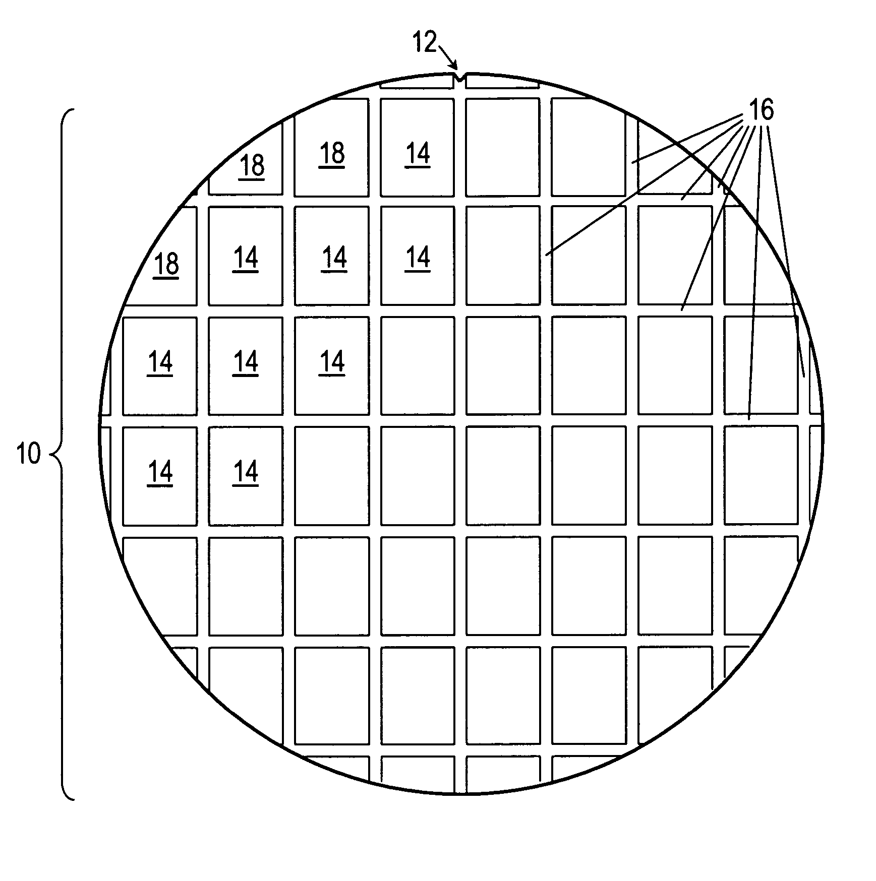
[0034] A method is disclosed for reducing stress concentration levels on the surfaces of a semiconductor wafer by exposure to a laser beam, thereby lowering the potential for chipping and cracking of the wafer during singulation. Referring briefly to FIG. 1, the active surface of a semiconductor wafer 10 typically includes scribe streets 16, sacrificial areas that are sawn thro...


PUM

PropertyMeasurementUnit
Widthaaaaaaaaaa
Areaaaaaaaaaaa

Abstract

A method for treating an area of a semiconductor wafer surface with a laser for reducing stress concentrations is disclosed. The wafer treatment method discloses treating an area of a wafer surface with a laser beam, wherein the treated area is ablated or melted by the beam and re-solidifies into a more planar profile, thereby reducing areas of stress concentration and stress risers that contribute to cracking and chipping during wafer singulation. Preferably, the treated area has a width less than that of a scribe street, but wider than the kerf created by a wafer dicing blade. Consequently, when the wafer is singulated, the dicing blade will preferably saw through treated areas only. It will be understood that the method of the preferred embodiments may be used to treat other areas of stress concentration and surface discontinuities on the wafer, as desired.

Description

BACKGROUND [0001] Modem-day semiconductor devices, commonly called integrated circuits, are fabricated on semiconductor wafers, and the wafers are then diced into grids, separating the integrated circuits into individual dies prior to final assembly. Integrated circuits are typically constructed at the surface of a wafer sliced from a single-crystal silicon ingot, although other semiconductors such as gallium arsenide and germanium are also used. Individual circuit elements, which form integrated circuits, are fabricated on and into the wafer surface, or substrate. [0002] The electrical conduction between appropriate circuit elements, and required electrical isolation between other circuit elements, is then established using alternating layers of appropriately patterned conductors and insulators. Substantially vertical, conductive tunnels called “vias” pass through insulating layers as needed to form conductive pathways between adjacent conductive layers. The creation of circuit ele...

Claims


Application Information

Patent Timeline
IPC IPC(8): B23K26/00B23K26/40H01L21/268H01L21/301H01L21/302H01L21/336H01L21/78
CPCB23K26/0075B23K26/4075H01L21/02016H01L21/268H01L21/302H01L2924/0002H01L21/78Y10S438/928H01L2924/00B23K26/40B23K26/3576B23K2103/50
Inventor MAHLE, RICHARD L.SAKAKINI, PETER J.
Owner TEXAS INSTR INC
Why Eureka
Try Eureka