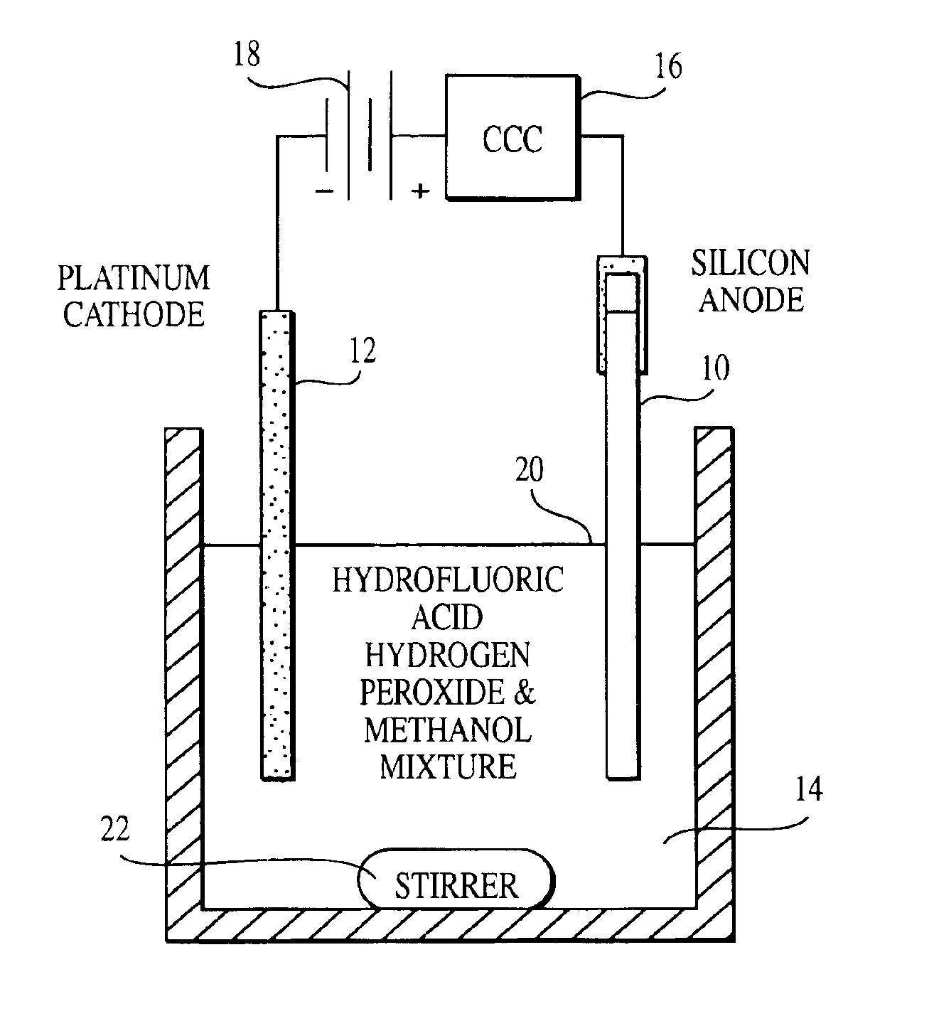
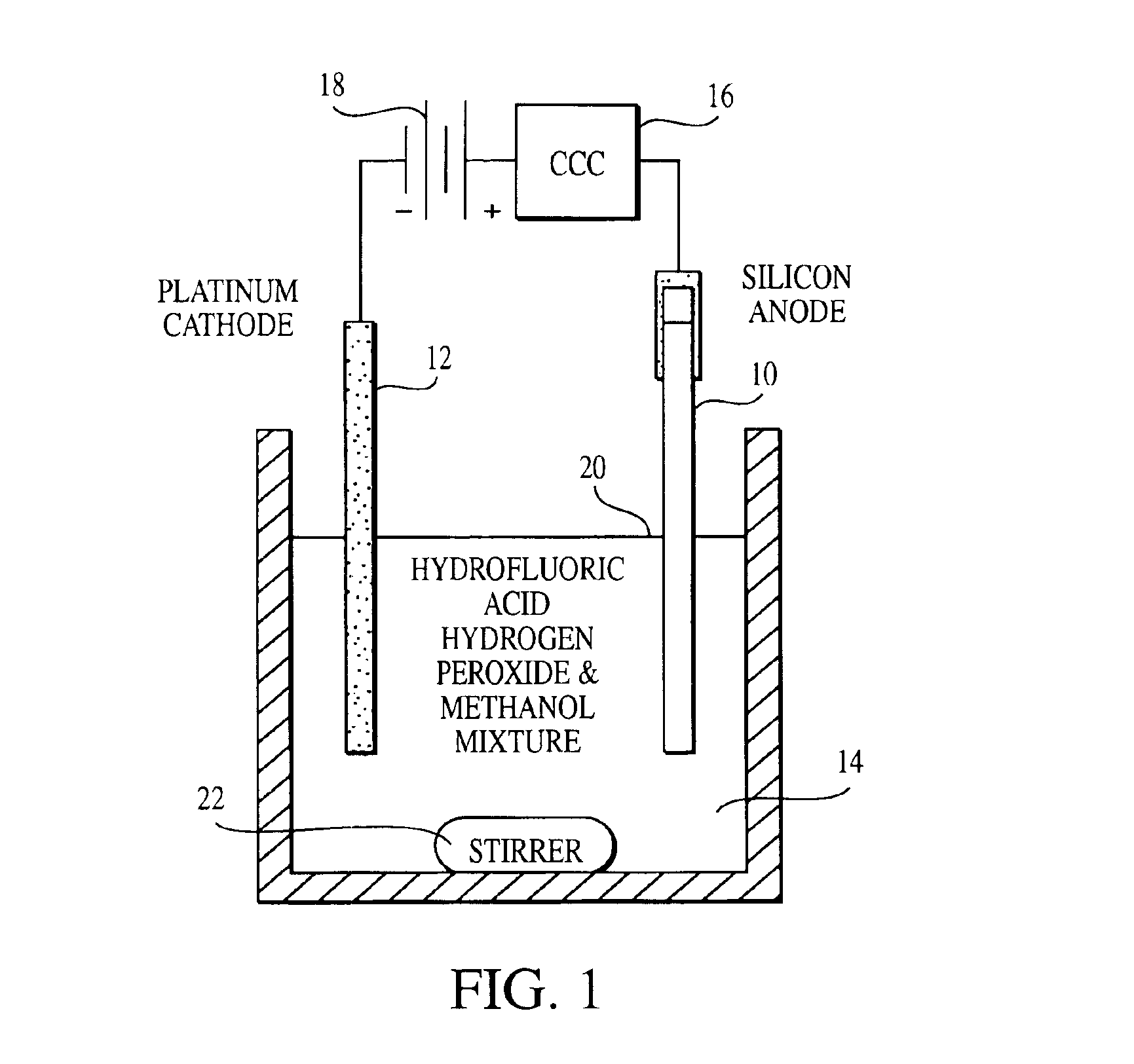
Silicon nanoparticle and method for producing the same
Inactive Publication Date: 2005-01-25
THE BOARD OF TRUSTEES OF THE UNIV OF ILLINOIS
View PDF23 Cites 60 Cited by
Summary
Abstract
Description
Claims
Application Information
AI Technical Summary
This helps you quickly interpret patents by identifying the three key elements:
Problems solved by technology
Method used
Benefits of technology
[0013]A method for producing the silicon nanoparticles of the invention is a gradual advancing electrochemical etch of bulk silicon. This may be followed by separation of nanoparticles from the surface of the silicon. Once separated, various methods may be employed to form plural nanoparticles into crystals,
Problems solved by technology
The understanding of bulk silicon, as well as atomic silicon, has limited the application of
Method used
Image
Click on the blue label to locate the original text in one second.
Reading with bidirectional positioning of images and text.
Examples
Embodiment Construction
ally illustrates a silicon nanoparticle based single electron transistor, optimized to work at high temperature;
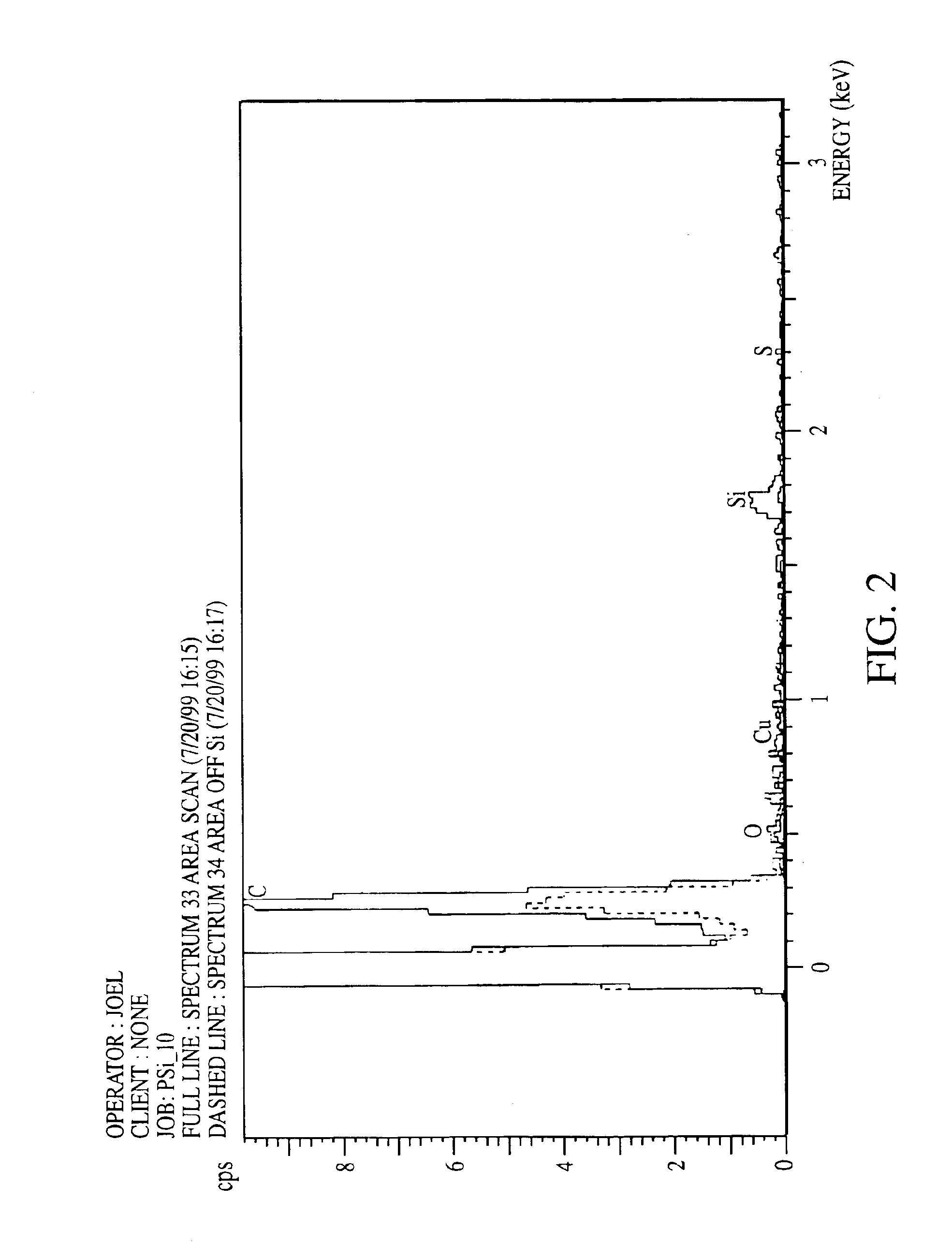
[0033]FIGS. 19a and 19b are the luminescence images of a 132×132 μm silicon nanoparticle section prior to separation from the wafer, respectively, taken at an average intensity of 5.7×10⁵ and 8×10⁵ W / cm2 (at 780 nm wavelength);
[0034]FIG. 20 plots the emission intensity for several of the individual bright spots seen in FIG. 19, as a function of the incident intensity;
[0035]FIG. 21 is a luminescent image of a silicon nanoparticle section prior to separation from the wafer and passivated with a high quality oxide;
[0036]FIGS. 22a and 22b give luminescence images a sample taken at an incident average power in CW mode at 820 nm respectively focused to 6.7×10⁶ and 8.3×10⁶ W / cm2;
[0037]FIG. 23 plots the development of the CW power pumping curves of the integrated emission from the 132×132 μm sample of FIG. 22;
[0038]FIG. 24a is a power pumping curve of the emission as a function of...
PUM
Abstract
Highly uniform 1 nm silicon nanoparticles are provided by the invention. The nanoparticles exhibit beneficial properties. They are a source of stimulated emissions. They may be suspended in liquids, and solids. They can be formed into crystals, colloids and films. The nanoparticles of the invention are about 1 nm having about only one part in one thousand greater than 1 nm. A method for producing the silicon nanoparticle of the invention is a gradual advancing electrochemical etch of bulk silicon. Separation of nanoparticles from the surface of the silicon may also be conducted. Once separated, various methods may be employed to form plural nanoparticles into colloids, crystals, films and other desirable forms. The particles may also be coated or doped.
Description
PRIORITY CLAIM[0002]This application is a continuation of application Ser. No. 09 / 426,389, filed Oct. 22, 1999 now U.S. Pat. No. 6,585,947 B1, and claims priority under 35 U.S.C. §120.REFERENCE TO RELATED APPLICATIONS[0003]This application is related to and incorporates by reference the following copending applications to Nayfeh et al:[0004]Ser. No. 09 / 781,147, entitled SILICON NANOPARTICLE ELECTRONIC SWITCHES, filed on Feb. 9, 2001;[0005]Ser. No. 09 / 572,121 entitled SILICON NANOPARTICLE MICROCRYSTAL NONLINEAR OPTICAL DEVICES, filed on May 17, 2000;[0006]Ser. No. 09 / 496,506 entitled SILICON NANOPARTICLE FIELD EFFECT TRANSISTOR AND TRANSISTOR MEMORY DEVICE, filed on Feb. 2, 2000;[0007]Ser. No. 09 / 426,204 entitled SILICON NANOPARTICLE STIMULATED EMISSION DEVICES, filed on Oct. 25, 1999; and now U.S. Pat. No. 6,597,496 B1 and[0008]U.S. patent application Nayfeh et al., Ser. No. 09 / 990,250, entitled FAMILY OF DISCRETELY SIZED SILICON NANOPARTICLES AND METHOD FOR PRODUCING THE SAME, file...
Claims
Application Information
Patent Timeline
Application Date:The date an application was filed.
Publication Date:The date a patent or application was officially published.
First Publication Date:The earliest publication date of a patent with the same application number.
Issue Date:Publication date of the patent grant document.
PCT Entry Date:The Entry date of PCT National Phase.
Estimated Expiry Date:The statutory expiry date of a patent right according to the Patent Law, and it is the longest term of protection that the patent right can achieve without the termination of the patent right due to other reasons(Term extension factor has been taken into account ).
Invalid Date:Actual expiry date is based on effective date or publication date of legal transaction data of invalid patent.