Active matrix type display device

a display device and active matrix technology, applied in the direction of static indicating devices, identification means, instruments, etc., can solve the problems of large area occupied by wiring in the region between rows, complex wiring undulation, and increased manufacturing cost, so as to minimize the length of wiring and maximize the emission region of each pixel. , the effect of reducing manufacturing cos

Inactive Publication Date: 2005-01-25
SANYO ELECTRIC CO LTD
View PDF9 Cites 18 Cited by
  • Summary
  • Abstract
  • Description
  • Claims
  • Application Information

AI Technical Summary

Benefits of technology

[0018]The present invention was conceived to solve the problem described above, and an object of the present invention is to simplify the wiring pattern in an active matrix type display device utilizing an organic EL element or the like.
[0022]With the arrangements of the driving power supply line as described above, it is possible to achieve a very simple wiring pattern between adjacent rows in a matrix without adversely affecting other circuit elements electrically due to the presence of the driving power supply line, such as, for example, generation of a parasitic capacitance. In addition, although the driving power supply line crosses within the pixel region from the second side to the first side, by employing a pattern in which the driving power supply line extends through a region between the switching thin film transistor and the element to be driven in a direction, for example, along the extension direction of the selection line as described above, it is possible to eliminate a diagonally extending portion of a wiring which tends to reduce the wiring efficiency in a matrix arrangement. Therefore, it is possible to improve the wiring efficiency and to increase the emission region of the pixel.
[0024]The connection region between the data line and the switching thin film transistor can be provided, for example, on a second side of the pixel in order to prevent obstruction by the driving power supply line. The element driving thin film transistor formed on the first side can be connected to the driving power supply line extending across from the second side to the first side. With such a configuration, for example, even with a delta arrangement it is not necessary to provide a special bypass wiring for the driving power supply line or to provide a wiring in a diagonal direction between the rows. As a result, the wiring pattern of the driving power supply line can be simplified and the wiring length can be shortened.
[0030]Even when it is necessary to form the data line and the driving power supply line in a region between pixel regions arranged in a matrix form or undulated within a pixel region, by employing a layout in which the two lines do not intersect, it is possible to form these lines simultaneously using the same material, to thereby allow combination of the manufacturing processes which is advantageous in terms of reducing manufacturing cost, etc.
[0031]According to the present invention, even when the pixels of the same color are arranged to be shifted by a predetermined pitch such as in a delta arrangement, wiring for a data line for supplying a data signal to each pixel and for a driving power supply line for supplying power to each pixel can be provided in a simple manner. In particular, also for the wiring pattern of the driving power supply line, it is possible to minimize the wiring length similar to the data line and, thus, it is possible to maximize the emission region of each pixel and to realize bright, high resolution color display devices.

Problems solved by technology

However, in an active matrix type organic EL display device, as shown in FIG. 1, a data line DL and a driving power supply line VL must be connected to each pixel in the column direction and, thus, when the delta arrangement is employed the wiring becomes more complicated than in a comparable LCD.
However, as is clear from FIG. 2, the wiring undulates in a complex manner among the rows and the area occupied by the wiring in the region between the rows is large.
When the area occupied by the wiring is large as in this case, the emission region (formation region of the organic EL element) is significantly limited on a substrate having a limited area, and, thus, improvements in aperture ratio cannot be achieved, that is, bright display cannot be produced.
Therefore, when the wiring resistance of the driving power supply line 45 is increased, there is a problem in that the pixels located at positions farther away from the driving power supply will exhibit lower emission brightness because of the voltage drop caused by the wiring resistance of the longer driving power supply line.

Method used


Image

  • Active matrix type display device
  • Active matrix type display device
  • Active matrix type display device

Examples


Embodiment Construction

the emission region of each pixel and to realize bright, high resolution color display devices.

BRIEF DESCRIPTION OF THE DRAWINGS

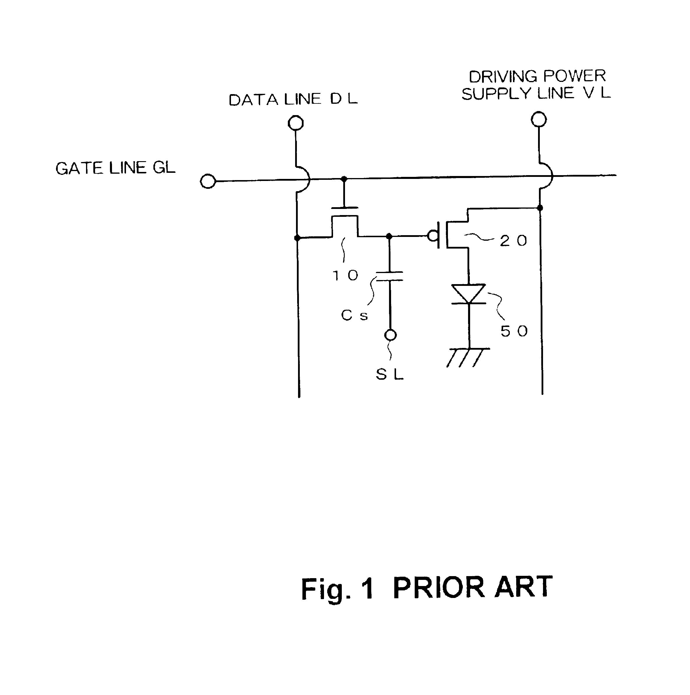
[0032]FIG. 1 is a diagram showing a circuit structure of a pixel of an active matrix type organic EL display device.

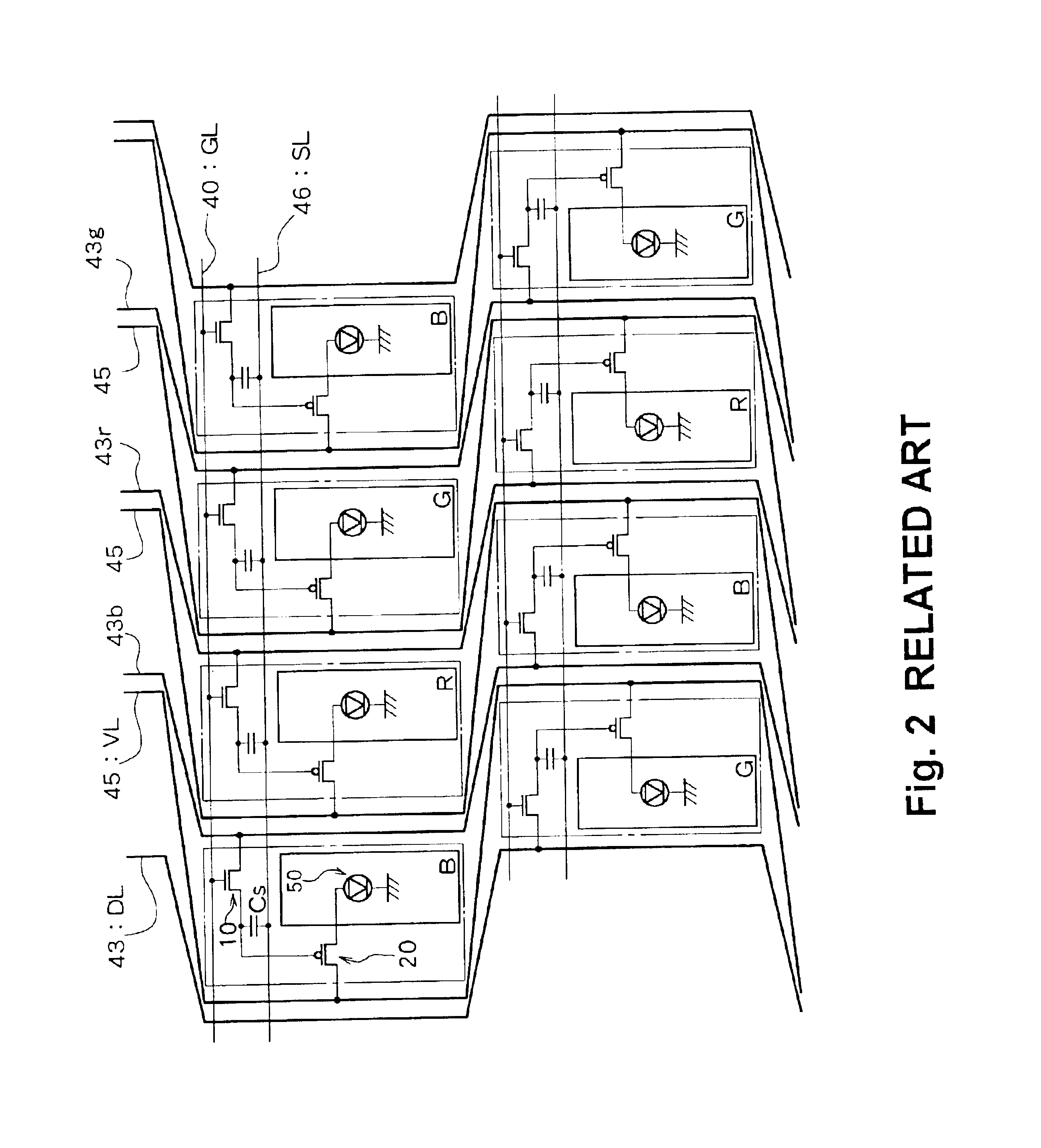
[0033]FIG. 2 is a diagram showing a predicted example layout of an active matrix type organic EL display device employing a delta arrangement.

[0034]FIG. 3 is a schematic diagram showing an arrangement of pixels in a preferred embodiment of the present invention.

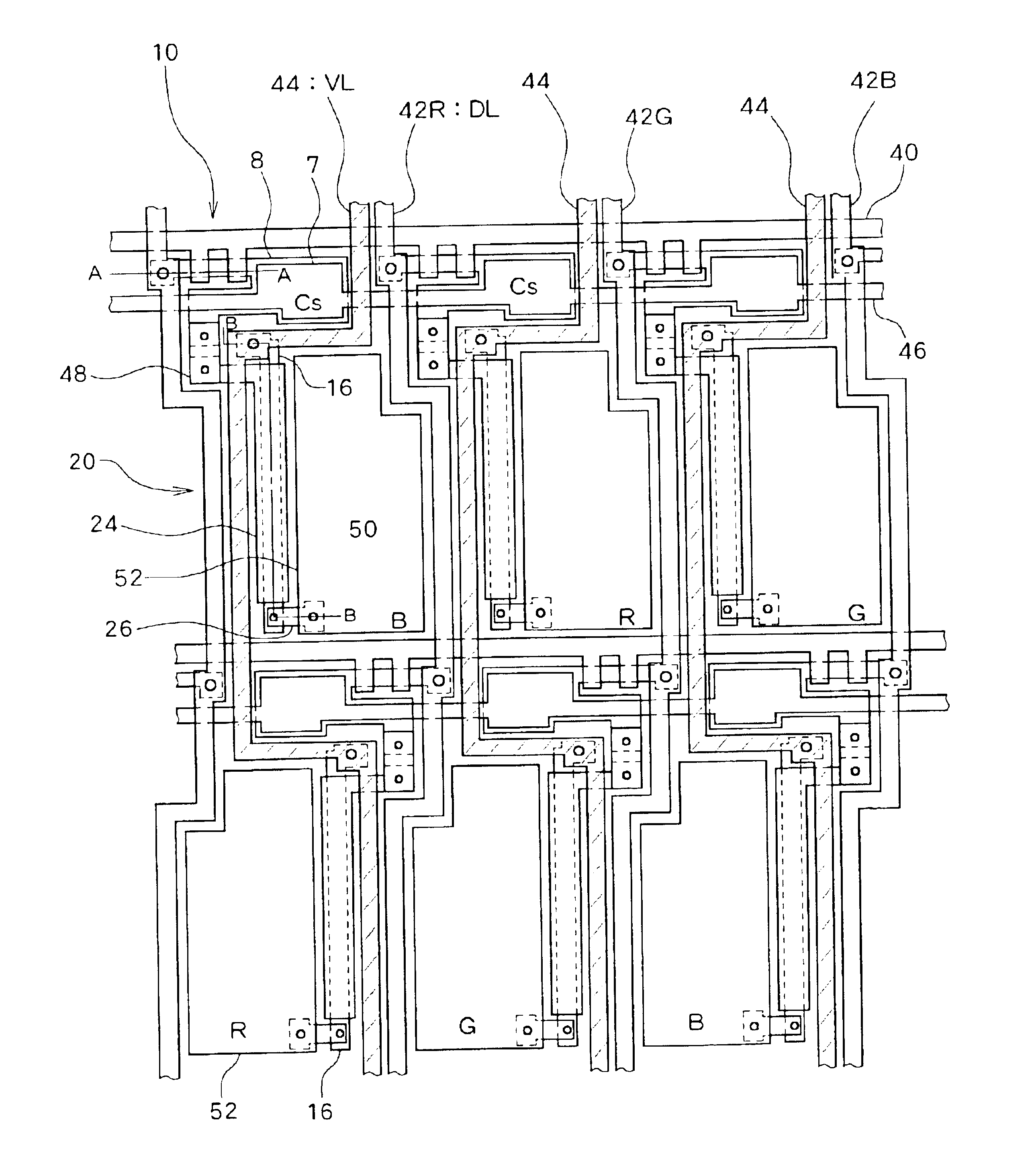
[0035]FIG. 4 is a planer diagram showing in more detail the arrangement shown in FIG. 3.

[0036]FIGS. 5A and 5B are cross sectional diagrams respectively showing cross sections along the A—A line and B—B line in FIG. 4.

DESCRIPTION OF PREFERRED EMBODIMENT

[0037]The preferred embodiment of the present invention (hereinafter referred to simply as the “embodiment”) will now be described referring to the drawings.

[0038]FIG. 3 shows a pixel layout of an active matrix type EL display device havin...


PUM


Abstract

An active matrix type display device comprising a plurality of pixels arranged in a matrix form, wherein each of the plurality of pixels comprises a display element, a second TFT for supplying power from a driving power supply line to the display element, and a first TFT for controlling the second TFT based on a data signal supplied from a data line when selected, and the driving power supply line extends across the pixel region. More specifically, of opposing first and second sides of a pixel, in a section where the first TFT is connected to the data line, the driving power supply line is placed on the second side, being the side opposite the data line, and in a section where the second TFT is connected to the driving power supply line, the driving power supply line is placed on the first side. In this manner, pixels provided in positions shifted for each row can be connected with a simple wiring layout.

Description

BACKGROUND OF THE INVENTION[0002]1. Field of the Invention[0003]The present invention relates to an active matrix type display device, and in particular to a layout of pixels and wiring in such a device.[0004]2. Description of the Related Art[0005]Electroluminescence (hereinafter referred to simply as “EL”) display devices in which a self-illuminating EL element is used for each pixel have advantages such as thinness and low power consumption, in addition to being self-illuminating. Because of these advantages, EL display devices have currently attracted much attention as an alternative display device for liquid crystal display devices (LCDs) and CRTs, and effort is therefore now being expended on their development.[0006]In particular, an active matrix type EL display device in which a switching element for individually controlling an EL element such as a thin film transistor (TFT) is provided in each pixel so that the EL element is driven individually for each pixel is highly expec...

Claims


Application Information

Patent Timeline
Patent Type & Authority Patents(United States)
IPC IPC(8): G09G3/32H01L27/12H01L51/50G09F9/00G09F9/30G09G3/20G09G3/30H01L21/77H01L27/32H05B33/00
CPCG09G3/3225H01L27/12H01L27/3211H01L27/3276G09G2300/0426G09G2300/0452G09G2300/0842H01L27/124G09G2320/0223H10K59/35H10K59/131H05B33/00
Inventor ANZAI, KATSUYA
Owner SANYO ELECTRIC CO LTD
Why Eureka
Try Eureka